+44 (0)24 7671 8970
More publications     •     Advertise with us     •     Contact us
 
News Article

Toshiba Starts Construction of Fab 6 and Memory R&D Centre in Japan


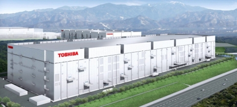
Artist's impression of Fab 6, Yokkaichi Operations
Toshiba Corporation has announced that it has started construction of a new state-of-the-art semiconductor fabrication facility, Fab 6, and a new R&D centre, the Memory R&D Center, at Yokkaichi Operations in Mie prefecture, Japan, the company's main memory production base.

Fab 6 will be dedicated to production of BiCS FLASH, Toshiba's innovative 3D Flash memory1. Like Fab 5, construction will take place in two phases, allowing the pace of investment to be optimized against market trends, with completion of Phase 1 scheduled for summer 2018. Toshiba will determine installed capacity and output targets and schedules by closely monitoring the market.

Toshiba will also construct a Memory R&D Centre adjacent to the new fab, with completion targeting December 2017. The facility will advance development of BiCS FLASH and new memories.

Toshiba is determined to enhance its competitiveness in the memory business by timely expansion of BiCS FLASH production in line with market trends, and to retain leadership in innovation in the memory business.

Purdue, imec, Indiana announce partnership
Resilinc partners with SEMI on supply chain resilience
NIO and NXP collaborate on 4D imaging radar deployment
Panasonic Industry digitally transforms with Blue Yonder
Global semiconductor sales decrease 8.7%
MIT engineers “grow” atomically thin transistors on top of computer chips
Keysight joins TSMC Open Innovation Platform 3DFabric Alliance
Leti Innovation Days to explore microelectronics’ transformational role
Quantum expansion
indie launches 'breakthrough' 120 GHz radar transceiver
Wafer fab equipment - facing uncertain times?
Renesas expands focus on India
Neuralink selects Takano Wafer Particle Measurement System
Micron reveals committee members
Avoiding unscheduled downtime in with Preventive Vacuum Service
NFC chip market size to surpass US$ 7.6 billion
Fujifilm breaks ground on new €30 million European expansion
Fraunhofer IIS/EAS selects Achronix embedded FPGAs
Siemens announces certifications for TSMC’s latest processes
EU Chips Act triggers further €7.4bn investment
ASE recognised for excellence by Texas Instruments
Atomera signs license agreement with STMicroelectronics
Gartner forecasts worldwide semiconductor revenue to decline 11% in 2023
CHIPS for America outlines vision for the National Semiconductor Technology Center
TSMC showcases new technology developments
Alphawave Semi showcases 3nm connectivity solutions
Greene Tweed to open new facility in Korea
Infineon enables next-generation automotive E/E architectures
Global AFM market to reach $861.5 million
Cepton expands proprietary chipset
Semtech adds two industry veterans to board of directors
Specialty gas expansion
×
Search the news archive

To close this popup you can press escape or click the close icon.
Logo
×
Logo
×
Register - Step 1

You may choose to subscribe to the Silicon Semiconductor Magazine, the Silicon Semiconductor Newsletter, or both. You may also request additional information if required, before submitting your application.


Please subscribe me to:


You chose the industry type of "Other"

Please enter the industry that you work in: