
AP&S International GmbH achieves competitive advantage by investing in a new ultra-high purity water system
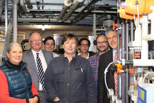
Since the beginning of 2017 the new UHPW system is in operation at the AP&S manufacturing facility in Donaueschingen. The system reduces the impurities of city residues up to the ultratrace level of <1ppb per cationic element. The system was installed by Haage & Elsässer (H&E) from Stuttgart, Germany. H&E provides industrial water treatment systems for more than 40 years and is one of the technological leaders in this field of UHPW concepts.
The main reason for the investment decision lies in the strong requirements on stability and purity of wet process applications in the semiconductor industry. Before a new wet process application can be used in production, it has to fulfill and demonstrate the required purity specifications. In practice, it means that before commissioning long-term rinsing and cleaning process at customer's fab is necessary, which is associated with time, resources and material consumption.
The AP&S process engineer team recognized that an optimization of this process-set up would bring considerable advantages for the customers. Thus the basic idea for the project was born. In 2016, the investment and installation of the new UHPW system followed.
Stefan Zuercher, Process Engineer at AP&S, sums up the most important advantages of the new water system: "Less water consumption and lower costs, associated with calculable risk of process hardware purity, which is monitored by on-line analytics, are the cornerstones of the new system. Additional new feature is that the used water can be recycled internally. The UHPW system has a storage capacity of 6-8 m³ of UHPW and a production capacity of 3m³ water per hour. The purified water is used for rinsing, cleaning and conditioning of the AP&S tools and the facility."
Prior to delivery to customers the AP&S tools are rinsed with the ultra-high purity water and qualified with optical particle counters (OLC's @ > 0.1 μm resolution). Samples for trace impurity measurements are checked for cation concentrations typically to levels <1ppb each. An ICP-MS or GF-AAS is used in an external laboratory close by.
The value add for each customer is, that tools can be much faster qualified, less effort is needed on site and defect density requirements for production output can be achieved much faster.
"The new water system enables AP&S to provide customer wet process applications, which meet the highest SC-technology standards", says Robert Preisser, Adjunct Professor at AP&S, who has initiated, specified and supported the project.
"With the implementation of this advanced water treatment technology, AP&S has put itself at the forefront of the medium-sized equipment providers for wet process solutions, which support the semiconductor and nanotechnology industries around the globe", adds CEO of AP&S Alexandra Laufer-Mueller.


