+44 (0)24 7671 8970
More publications     •     Advertise with us     •     Contact us
 
News Article

Silectra appoint new CEO

News

SILTECTRA GmbH, a technology specialist for kerf-less wafering, has a new CEO. Dr. Harald Binder is known as an expert in the semiconductor industry. His strategic goal is to prepare the company for entering the commercialization phase. He will work closely with Dr. Jan Richter, CTO, who has been responsible for technology and process development since 2011 and collaborated on more than 25 new patents since that time. Former CEO, Dr. Wolfgang Drescher, will join the Advisory Board and will continue to shape the company in his new role.

"Harald Binder is the industry expert we have been looking for. He brings many years of experience in strategic development and production optimization. It is precisely this experience that we need in order to take advantage of the imminent demand for power semiconductors and provide manufacturers with cost-effective wafering solutions," said Dr. Axel Thierauf, Partner of MIG Verwaltungs AG, whose MIG-Funds hold a majority stake in SILTECTRA GmbH.

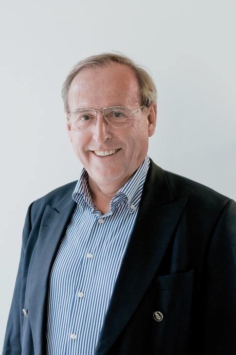
Dr. Harald Binder started his career in the atom physics sector in 1977. He then entered the semiconductor industry at Siemens Semiconductor, where he was involved in the DRAM activities for several years. He continued his career in different management roles at M+W Zander, a leading construction company for semiconductor manufacturing sites. From 2006 to 2008, he was CEO of centrotherm thermal solution AG. Afterwards he joined the world leading equipment manufacturer Applied Materials as Vice President and General Manager. In the last five years, he supported the business and strategy development of several companies in the semiconductor sector as an independent consultant.

SILTECTRA processes high-quality semiconducting material to create wafers for the chip industry without loss of material. The special laser process, which SILTECTRA has pioneered, is based on a chemical-physical process where thermal stress generates force that splits the material along the desired plane. Compared to conventional methods such as sawing, the process cuts material loss by more than 90%. SILTECTRA's technology is therefore particularly advantageous when very cost-intensive semiconductor materials such as silicon carbide are used.

"Depending on the material, the substrate allocates between 5 and 50 percent of the cost of a single device. Our COLD SPLIT technology makes the new chip generation for power electronics up to 15 to 20 percent less expensive. Those cost benefits will accelerate the market penetration of future applications like 5G, wireless charging or electro mobility," said the SILTECTRA CEO Dr. Harald Binder.

Since September 2016, SILTECRA has been operating a pilot process for cleaving semiconductor materials in Dresden. The company is currently developing a system and a relating process to meet high volume manufacturing requirements. That is expected to be available by Q3 2017 in the new SILTECTRA building.

Purdue, imec, Indiana announce partnership
Resilinc partners with SEMI on supply chain resilience
NIO and NXP collaborate on 4D imaging radar deployment
Panasonic Industry digitally transforms with Blue Yonder
Global semiconductor sales decrease 8.7%
MIT engineers “grow” atomically thin transistors on top of computer chips
Keysight joins TSMC Open Innovation Platform 3DFabric Alliance
Leti Innovation Days to explore microelectronics’ transformational role
Quantum expansion
indie launches 'breakthrough' 120 GHz radar transceiver
Wafer fab equipment - facing uncertain times?
Renesas expands focus on India
Neuralink selects Takano Wafer Particle Measurement System
Micron reveals committee members
Avoiding unscheduled downtime in with Preventive Vacuum Service
NFC chip market size to surpass US$ 7.6 billion
Fujifilm breaks ground on new €30 million European expansion
Fraunhofer IIS/EAS selects Achronix embedded FPGAs
Siemens announces certifications for TSMC’s latest processes
EU Chips Act triggers further €7.4bn investment
ASE recognised for excellence by Texas Instruments
Atomera signs license agreement with STMicroelectronics
Gartner forecasts worldwide semiconductor revenue to decline 11% in 2023
CHIPS for America outlines vision for the National Semiconductor Technology Center
TSMC showcases new technology developments
Alphawave Semi showcases 3nm connectivity solutions
Greene Tweed to open new facility in Korea
Infineon enables next-generation automotive E/E architectures
Global AFM market to reach $861.5 million
Cepton expands proprietary chipset
Semtech adds two industry veterans to board of directors
Specialty gas expansion
×
Search the news archive

To close this popup you can press escape or click the close icon.
Logo
×
Logo
×
Register - Step 1

You may choose to subscribe to the Silicon Semiconductor Magazine, the Silicon Semiconductor Newsletter, or both. You may also request additional information if required, before submitting your application.


Please subscribe me to:


You chose the industry type of "Other"

Please enter the industry that you work in: