
Stanford team reveals new properties of 2D semiconductors
Latest research on HfSe2 and ZrSe2 suggest they are promising materials for electronics of the future
Electrical engineers at Stanford University have identified two 2D compound semiconductors "“ HfSe2 and ZrSe2 "“ that share or even exceed some of silicon's desirable traits.
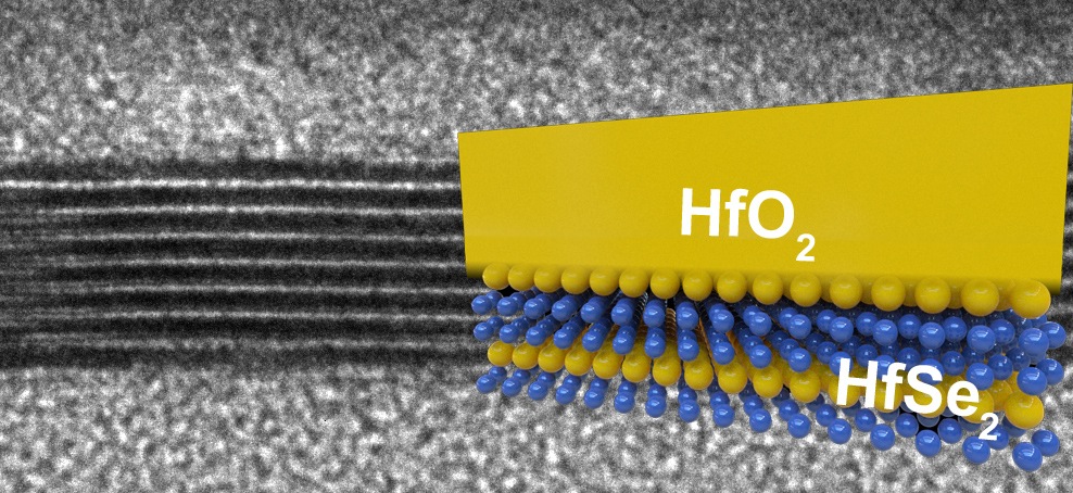
The materials can be shrunk to functional circuits just three atoms thick and they require less energy than silicon circuits. In addition, when exposed to oxygen during manufacturing they quickly form an insulating oxide or 'rust'.
Exposing silicon to oxygen during manufacturing gives chip-makers an easy way to isolate their circuitry by producing SiO2. Other semiconductors do not turn into good insulators when exposed to oxygen, so they must be layered with additional insulators, a step that introduces engineering challenges.
Both of the diselenides the Stanford group tested formed this high-quality insulating 'rust' layer when exposed to oxygen and in a way that is better than silicon, said Eric Pop, an associate professor of electrical engineering, who co-authored with post-doctoral scholar Michal Mleczko a paper that appears in the journal Science Advances. They form 'high-K' insulators, which enable lower power operation than is possible with silicon and its silicon oxide insulator.
As the Stanford researchers started shrinking the diselenides to atomic thinness, they realised that these ultrathin semiconductors had another advantage: the band gap energy needed to switch transistors on is in a just-right range. Too low and the circuits leak and become unreliable. Too high and the chip takes too much energy to operate and becomes inefficient. Both materials were in the same optimal range as silicon.
The diselenides can also be fashioned into circuits just three atoms thick, or about two-thirds of a nanometer."Engineers have been unable to make silicon transistors thinner than about 5nm, before the material properties begin to change in undesirable ways," Pop said.
The combination of thinner circuits and desirable high-K insulation means that these ultrathin semiconductors could be made into transistors ten times smaller than anything possible with silicon today."Silicon won't go away. But for consumers this could mean much longer battery life and much more complex functionality if these semiconductors can be integrated with silicon," Pop said.
More work to do
There is much work ahead. First, Mleczko and Pop must refine the electrical contacts between transistors on their ultrathin diselenide circuits. "These connections have always proved a challenge for any new semiconductor, and the difficulty becomes greater as we shrink circuits to the atomic scale," Mleczko said.
They are also working to better control the oxidised insulators to ensure they remain as thin and stable as possible. Last, but not least, only when these things are in order will they begin to integrate with other materials and then to scale up to working wafers, complex circuits and, eventually, complete systems."There's more research to do, but a new path to thinner, smaller circuits "“ and more energy-efficient electronics "“ is within reach," Pop said.
Additional Stanford contributors to this research include: Chaofan Zhang, Hye Ryoung Lee, Hsueh-Hui Kuo, Blanka Magyari-Köpe, Robert G. Moore, Zhi-Xun Shen, Ian R. Fisher, and Professor Yoshio Nishi.
The work was supported by the Air Force Office of Scientific Research (AFOSR), the National Science Foundation, Stanford Initiative for Novel Materials and Processes (INMP), the Department of Energy (DOE) Office of Basic Energy Sciences, Division of Material Sciences, and an NSERC PGS-D fellowship.


