
Flexible hybrid electronics "“ a new paradigm for semiconductors
Thin die being attached to flexible substrates at NextFlex
The limitations of rigid electronics The fundamentals of electronics manufacturing "“ packaged semiconductors and other components assembled onto printed circuit boards produced in high-temperature processes "“ have not changed for decades. This process results in durable, reliable systems and is widely available from numerous suppliers. The process is well suited for computing- and memory-intensive applications such as servers, communications systems, industrial process equipment and other installed systems.
As interest has increased in devices for Internet of Things (IoT) applications, the limitations of this approach have become apparent. Many of these devices must necessarily be thin and lightweight, and often must be flexible (to accommodate movement of the body or of systems) or conformable (to blend into curved structures). Packaged components on rigid circuit boards are not able to meet these requirements. The process has evolved somewhat with the development of rigid-flex circuitry, in which flexible circuit substrates provide a backbone of wiring with rigid multilayer circuit sections built up as modules where needed. This can enable some flexibility, but does not allow for the electronics to be fully integrated into clothing or other materials, or worn directly on the body.
Interest in flexible electronics has led many companies and research groups to pursue printed electronics, in which interconnect, passive devices, and even semiconductors are fabricated directly onto flexible substrates. These processes enable thin, lightweight, and flexible electronic devices. However, the use of printing or other additive processes to fabricate semiconductors has proven to be very limited, lagging the density achieved by photolithography by many orders of magnitude.
Getting electronics out of the box New forms of electronic manufacturing are required to create intelligent devices that can sense, take action, and communicate in real time while being integrated into the real world, whether that is on the human body, the surface of a vehicle, precious cargo in transit, or a robotic system. Flexible hybrid electronics (FHE) is an approach that utilizes electronic printing and other additive techniques in conjunction with bare semiconductor die to create thin, flexible circuits. Starting with a flexible substrate, such as plastic or polymer film, metal foil, fabric, paper, or even thin versions of glass or ceramic, low-temperature printing and additive processes can be used to create interconnects, sensors, antennas, passive components, and some active devices. Bare semiconductor die that have been thinned (to a thickness of 50 microns or less) are then integrated into the printed circuitry and the system is encapsulated.
The FHE approach provides significant benefits. Because it utilizes semiconductor devices, it enables system performance equivalent to rigid PCB solutions, which purely printed electronics approaches are not able to achieve. At the same time, the combination of flexible substrates, printing, and thinned semiconductor devices results in system form factors that can be bent, flexed, stretched and conformed to non-planar surfaces.
What does this mean for the silicon supply chain?
The FHE approach creates opportunities for semiconductor device and electronics manufacturers to address emerging applications that cannot be satisfied by existing assembly approaches. New products envisioned for human performance monitoring, patient monitoring, structural monitoring, preventative maintenance, asset tracking, integrated array antennas, soft robotics, and assistive technologies such as exoskeletons will not be possible using packaged semiconductors on printed circuit boards. By embracing FHE manufacturing, supply chain participants will be able to build new lines of business.
Because FHE processes are low temperature and additive in nature, manufacturing and assembly capabilities can be built as needed, and importantly, where they are needed. Also, FHE manufacturing can be scaled from prototyping to volume manufacturing as needed. Small-scale investments can enable rapid prototyping capabilities, while larger investments will enable manufacturing close to customers and markets.
Taking advantage of the potential of FHE manufacturing will require changes to the semiconductor supply chain. The existing supply chain is built on the assumption that all semiconductor devices are packaged and assembled onto circuit boards. The development of FHE manufacturing requires that bare semiconductor die, in many cases thinned to 50 microns or less, are available for assembly. Equipment and processes for thinning wafers up to 300 mm are available, but in most cases this equipment is embedded in a supply chain that involves thinning, singulation, and packaging. To take advantage of the new markets enabled by FHE manufacturing, semiconductor device manufacturers will need to either develop or support a sales and distribution network for thin die, or to sell fully manufactured wafers directly to FHE manufacturers, who would then thin and singulate the wafers.
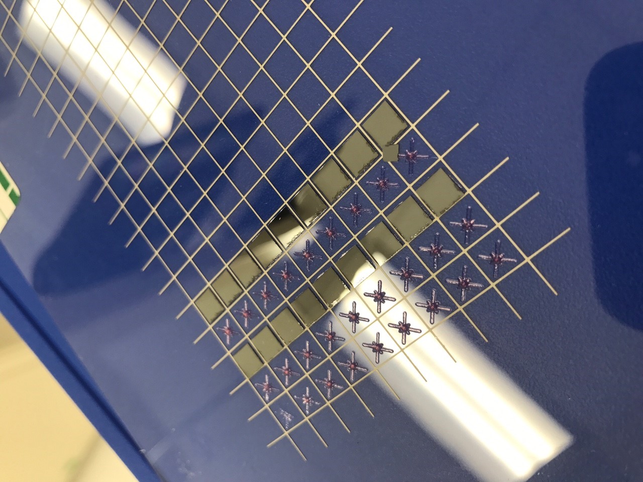
Another area of opportunity will be in assembly equipment. Unlike surface-mount technology, in which packaged components are soldered to circuit boards at high temperatures, FHE assembly involves placement and attachment of thin, bare semiconductor die (and possibly other components) onto thin sheets of polymers or other materials at low temperature; see Figure 1 for an example. This requires specialized handling and bonding techniques not widely available now.
NextFlex: enabling FHE manufacturing through collaboration
Many of the fundamental materials and technologies for FHE, such as thin substrates, high-resolution printing, and bare die assembly, already exist in some form. What has been missing is an effort to integrate these disparate technologies, demonstrate their feasibility, and create the standard processes, design rules, and other underlying capabilities required for a robust supply chain. This drove the creation of NextFlex in 2015 under a contract with the Department of Defense. By bringing together dozens of companies, universities, research centers, and government agencies into a public-private collaborative research consortium, NextFlex is creating the forum to tackle common FHE industry challenges. By creating roadmaps for manufacturing processes and application needs, identifying key performance gaps, and supporting shared research to address the gaps in a pre-competitive forum, NextFlex is accelerating the creation of a new capability for flexible hybrid electronics manufacturing.

Figure 2 "“ Meyer Burger PiXDRO digital printer in the NextFlex Technology Hub, San Jose, Calif.

Paul Semenza, Director of Commercialization, NextFlex


