
Samsung Image Sensor Enables Mobile Devices to "˜Slow Down' Time
Samsung Electronics has introduced the newest addition to its ISOCELL image sensor family, the 3-stack ISOCELL Fast 2L3. The 1.4-micrometer (μm) 12-megapixel (Mp) image sensor with integrated dynamic random access memory (DRAM) delivers fast data readout speeds to capture both rapid movements in super-slow motion and sharper still photographs with less noise and distortion.
"Samsung's ISOCELL image sensors have made great leaps over the generations, with technologies such as ISOCELL for high color fidelity and Dual Pixel for ultra-fast autofocusing, bringing the smartphone camera ever closer to DSLR-grade photography," said Ben K. Hur, vice president of System LSI marketing at Samsung Electronics. "With an added DRAM layer, Samsung's new 3-stack ISOCELL Fast 2L3 will enable users to create more unique and mesmerizing content."
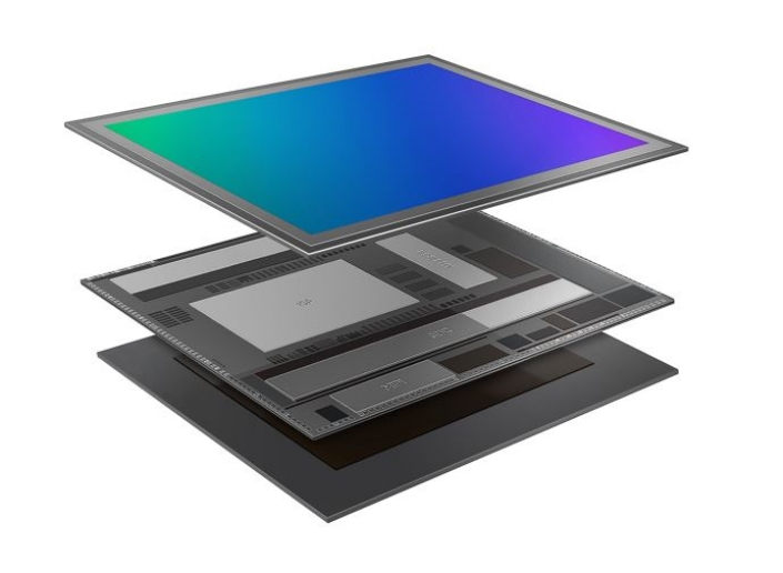
Conventional image sensors are constructed with two silicon layers; a pixel array layer that converts light information into an electric signal, and an analog logic layer that processes the electric signal into digital code. The digital code is then sent via MIPI interface to the device's mobile processor for further image tuning before being saved to the device's DRAM. While all these steps are done instantaneously to implement features like zero-shutter lag, capturing smooth super-slow-motion video requires image readouts at a much higher rate.
Delivering an advanced solution, the Samsung ISOCELL Fast 2L3 is a high speed 3-stack CMOS image sensor designed with the company's two-gigabit (Gb) LPDDR4 DRAM attached below the analog logic layer. With the integration, the image sensor can temporarily store a larger number of frames taken in high speed quickly onto the sensor's DRAM layer before sending frames out to the mobile processor and then to the device's DRAM. This not only allows the sensor to capture a full-frame snapshot at 1/120 of a second but also to record super-slow motion video at up to 960 frames per second (fps). With 960fps recording, which is 32 times the typical filming speed (30fps), recording moments such as a child hitting his or her first game-winning homerun, a baby taking his or her first step, or a friend doing a gazelle flip on a skateboard becomes much more dramatic.
In addition to super slow motion video, fast readout can hugely enhance the photography experience. Since the sensor captures an image at very high speeds, it significantly reduces the "˜jello-effect,' or image distortion, when taking a picture of fast-moving objects, for example helicopter rotor blades. By storing multiple frames in the split of a second, the sensor can support 3-Dimensional Noise Reduction (3DNR) for clearer pictures when shooting in low-light, as well as real time high-dynamic-range (HDR) imaging, and detect even the slightest hint of movement for automatic instant slow-motion recording.
The image sensor is also equipped with Dual Pixel technology, which allows each and every one of the 12-million pixels of the image sensor to employ two photodiodes that respectively work as a phase detection auto-focus (PDAF) agent. With ultra-fast auto-focus in any lighting condition, it will be harder to miss capturing important moments before they pass by. The Samsung ISOCELL Fast 2L3 is currently in mass production.


