+44 (0)24 7671 8970
More publications     •     Advertise with us     •     Contact us
 
News Article

Atotech's new horizontal activator pre dip for fine line applications

News

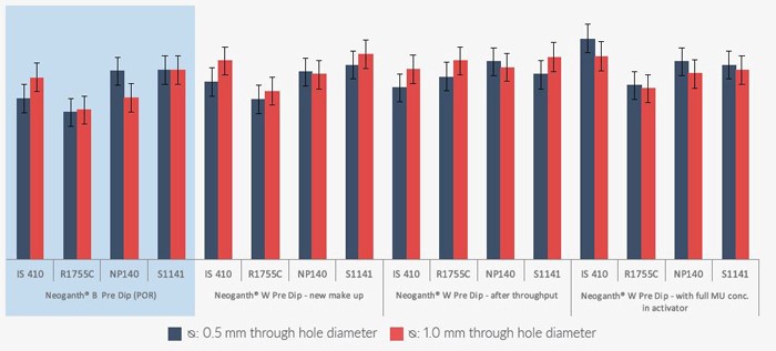
Coverage performance comparison on 4 different base materials (Isola IS410,Panasonic R1755C, Nanya NP140,Shengyi S1141) after new make-up, throughput and with maximum drag-in of Neoganth W Pre Dip into the subsequent activator bath

Neoganth W Pre Dip is Atotech's new process for the desmear and metallization (PTH) process step for fine line HDI and package substrate applications. The new pre dip assures higher yield rates due to a significantly reduced occurrence of short circuits.

The trend for ever smaller lines and spaces in advanced HDI boards for mobile applications continues. Lines and spaces (L/S) will be reduced to 25/25 µm by 2019. The trend was made possible by manufacturing technologies such as modified semi-additive processes (mSAP) and advanced modified semi-additive processes (amSAP). With this minimization comes the need for new PORs (process of record), which offer significant technical advantages over existing ones.

Atotech's newly developed Neoganth W Pre Dip is a low foaming activator pre dip designed for horizontal transportation mode such as in Atotech's Uniplate LB line. The process leads to a significant reduction in particle formation thereby enabling higher yield rates in fine line production. A key feature to achieve this is its alkaline pH.

Customer data has shown that using Neoganth W Pre Dip reduces the occurrence of short circuits in the process by up to 50% compared to competitive products. At the same time, the process provides excellent coverage performance while significantly reducing foaming behaviour.

Purdue, imec, Indiana announce partnership
Resilinc partners with SEMI on supply chain resilience
NIO and NXP collaborate on 4D imaging radar deployment
Panasonic Industry digitally transforms with Blue Yonder
Global semiconductor sales decrease 8.7%
MIT engineers “grow” atomically thin transistors on top of computer chips
Keysight joins TSMC Open Innovation Platform 3DFabric Alliance
Leti Innovation Days to explore microelectronics’ transformational role
Quantum expansion
indie launches 'breakthrough' 120 GHz radar transceiver
Wafer fab equipment - facing uncertain times?
Renesas expands focus on India
Neuralink selects Takano Wafer Particle Measurement System
Micron reveals committee members
Avoiding unscheduled downtime in with Preventive Vacuum Service
NFC chip market size to surpass US$ 7.6 billion
Fujifilm breaks ground on new €30 million European expansion
Fraunhofer IIS/EAS selects Achronix embedded FPGAs
Siemens announces certifications for TSMC’s latest processes
EU Chips Act triggers further €7.4bn investment
ASE recognised for excellence by Texas Instruments
Atomera signs license agreement with STMicroelectronics
Gartner forecasts worldwide semiconductor revenue to decline 11% in 2023
CHIPS for America outlines vision for the National Semiconductor Technology Center
TSMC showcases new technology developments
Alphawave Semi showcases 3nm connectivity solutions
Greene Tweed to open new facility in Korea
Infineon enables next-generation automotive E/E architectures
Global AFM market to reach $861.5 million
Cepton expands proprietary chipset
Semtech adds two industry veterans to board of directors
Specialty gas expansion
×
Search the news archive

To close this popup you can press escape or click the close icon.
Logo
×
Logo
×
Register - Step 1

You may choose to subscribe to the Silicon Semiconductor Magazine, the Silicon Semiconductor Newsletter, or both. You may also request additional information if required, before submitting your application.


Please subscribe me to:


You chose the industry type of "Other"

Please enter the industry that you work in: