
EV GROUP accelerates 3D-IC packaging roadmap
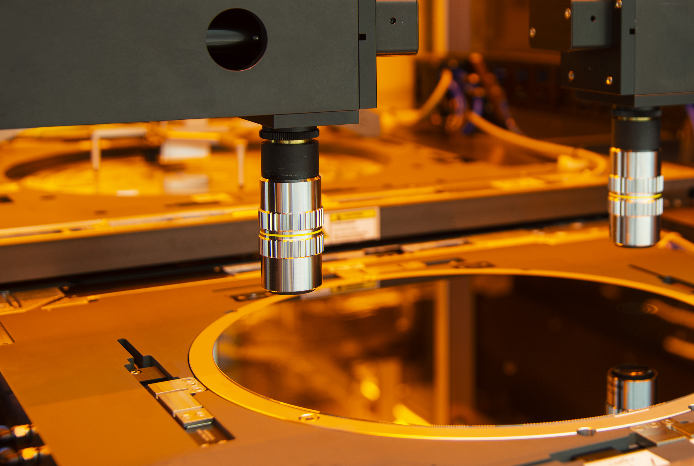
EV Group (EVG), a supplier of wafer bonding and lithography equipment for the MEMS, nanotechnology and semiconductor markets, has unveiled the new SmartView NT3 aligner, which is available on the company's industry benchmark GEMINI FB XT integrated fusion bonding system for high-volume manufacturing (HVM) applications. Developed specifically for fusion and hybrid wafer bonding, the SmartView NT3 aligner provides sub-50-nm wafer-to-wafer alignment accuracy"”a 2-3X improvement"”as well as significantly higher throughput (up to 20 wafers per hour) compared to the previous-generation platform.
With the new SmartView NT3 aligner, the GEMINI FB XT provides integrated device manufacturers, foundries and outsourced semiconductor assembly and test providers (OSATs) with wafer bonding performance that is unmatched in the industry and can meet their future 3D-IC packaging requirements. Applications enabled by the enhanced GEMINI FB XT include memory stacking, 3D systems on chip (SoC), backside illuminated CMOS image sensor stacking, and die partitioning.
Wafer Bonding an Enabling Process for 3D Device Stacking
Vertical stacking of semiconductor devices has become an increasingly viable approach to enabling continuous improvements in device density and performance. Wafer-to-wafer bonding is an essential process step to enable 3D stacked devices. However, tight alignment and overlay accuracy between the wafers is required to achieve good electrical contact between the interconnected devices on the bonded wafers, as well as to minimize the interconnect area at the bond interface so that more space can be made available on the wafer for producing devices. The constant reduction in pitches that are needed to support component roadmaps is fueling tighter wafer-to-wafer bonding specifications with each new product generation.
"At imec, we believe in the power of 3D technology to create new opportunities and possibilities for the semiconductor industry, and we are devoting a great deal of energy into improving it," stated Eric Beyne, imec fellow and program director 3D system integration. "One area of particular focus is wafer-to-wafer bonding, where we are achieving excellent results in part through our work with industry partners such as EV Group. Last year, we succeeded in reducing the distance between the chip connections, or pitch, in hybrid wafer-to-wafer bonding to 1.4 microns, which is four times smaller than the current standard pitch in the industry. This year we are working to reduce the pitch by at least half again."
"EVG's GEMINI FB XT fusion bonding system has consistently led the industry in not only meeting but exceeding performance requirements for advanced packaging applications, with key overlay accuracy milestones achieved with several industry partners within the last year alone," stated Paul Lindner, executive technology director, EV Group. "With the new SmartView NT3 aligner specifically engineered for the direct bonding market and added to our widely adopted GEMINI FB XT fusion bonder, EVG once again redefines what is possible in wafer bonding"”helping the industry to continue to push the envelope in enabling stacked devices with increasing density and performance, lower power consumption and smaller footprint."
The GEMINI FB XT fusion bonder with new SmartView NT3 aligner is available for customer demonstrations and testing. More information on the product can be found on EVG's website at https://www.evgroup.com/en/products/bonding/integrated_bonding/geminifb/.
EVG will showcase the GEMINI FB XT with new SmartView NT3 aligner, along with its complete suite of wafer bonding, lithography and resist processing solutions for advanced packaging applications, at SEMICON West, to be held July 10-12 at the Moscone Convention Center in San Francisco, Calif. Attendees interested in learning more can visit EVG at Booth #623 in the South Hall.
In addition, Dr. Thomas Uhrmann, director of business development at EV Group, will highlight the GEMINI FB XT and other developments in wafer bonding in his presentation "Collective Bonding for Heterogeneous Integration in Advanced Packaging" at the Meet the Experts Theater Smart Manufacturing Pavilion at SEMICON West on Thursday, July 12 from 3:00-3:30 p.m. in the South Hall.


