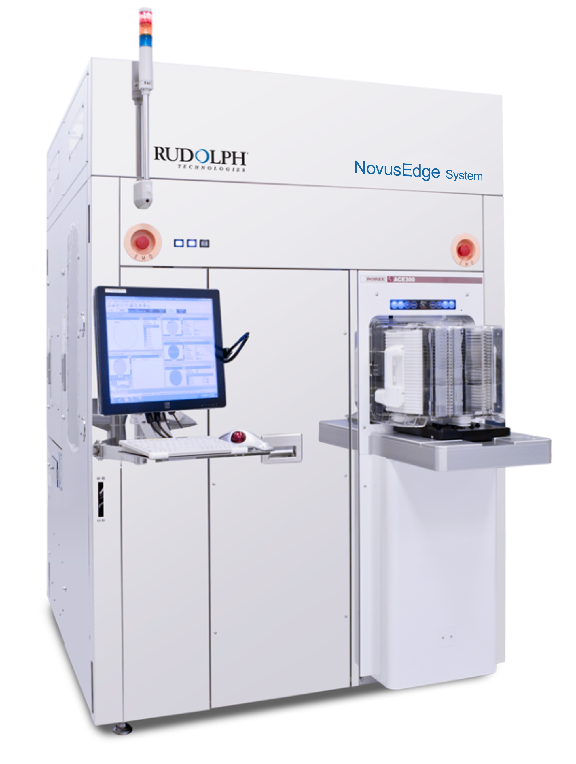
Rudolph Technologies announce the receipt of over $12 million in new orders

Rudolph Technologies has announced the receipt of over $12 million in new orders for its recently-released NovusEdge system for edge and backside inspection on bare silicon wafers. The new orders are for capacity expansions at our existing customers as well as orders from two additional large wafer manufacturers based in Asia. These orders are in addition to the $3M previously announced and will ship throughout calendar year 2019.
“With these orders Rudolph has expanded its customer base to include the top wafer suppliers with over 75% of the bare wafer market share,” said Mike Plisinski, Rudolph Technologies’ CEO. “We believe the early acceptance of these new systems is being driven by the accelerating demand for high-quality bare silicon wafers for sub 20nm nodes. To meet that demand customers require an inspection solution with increased sensitivity on the wafer edge and backside. The Rudolph team worked closely with bare wafer manufacturers in order to introduce a new product with compelling capabilities and value of ownership. As the rate of die shrinks slows at the advanced nodes, more wafers are required to make enough die to meet growing market demand, especially for advanced memory and logic chips.”
Chips and micro-fractures at the edge readily propagate as cracks into active areas of the wafer, especially when the wafer is thinned. Backside contamination can distort the frontside of the wafer during lithography, consuming focus budgets that are already thin and will become even thinner with the adoption of EUV lithography.
Edge and backside inspection have requirements that are very different from conventional frontside inspection. The NovusEdge EBI (Edge, Backside Inspection) system’s image-based approach provides full coverage of near-edge, bevel and apex regions, both top and bottom. Compared to existing technology, it is faster, more sensitive and better at classifying types of defects, especially for the complex shapes and curvatures at the notch. Backside inspection can use the same light scattering techniques used on the frontside but requires special handling capabilities to avoid contacting or contaminating the frontside. In all cases, sophisticated software provides analysis and automatic defect classification.


