+44 (0)24 7671 8970
More publications     •     Advertise with us     •     Contact us
 
News Article

Atomic-scale memristive devices: small, smart and scalable

News

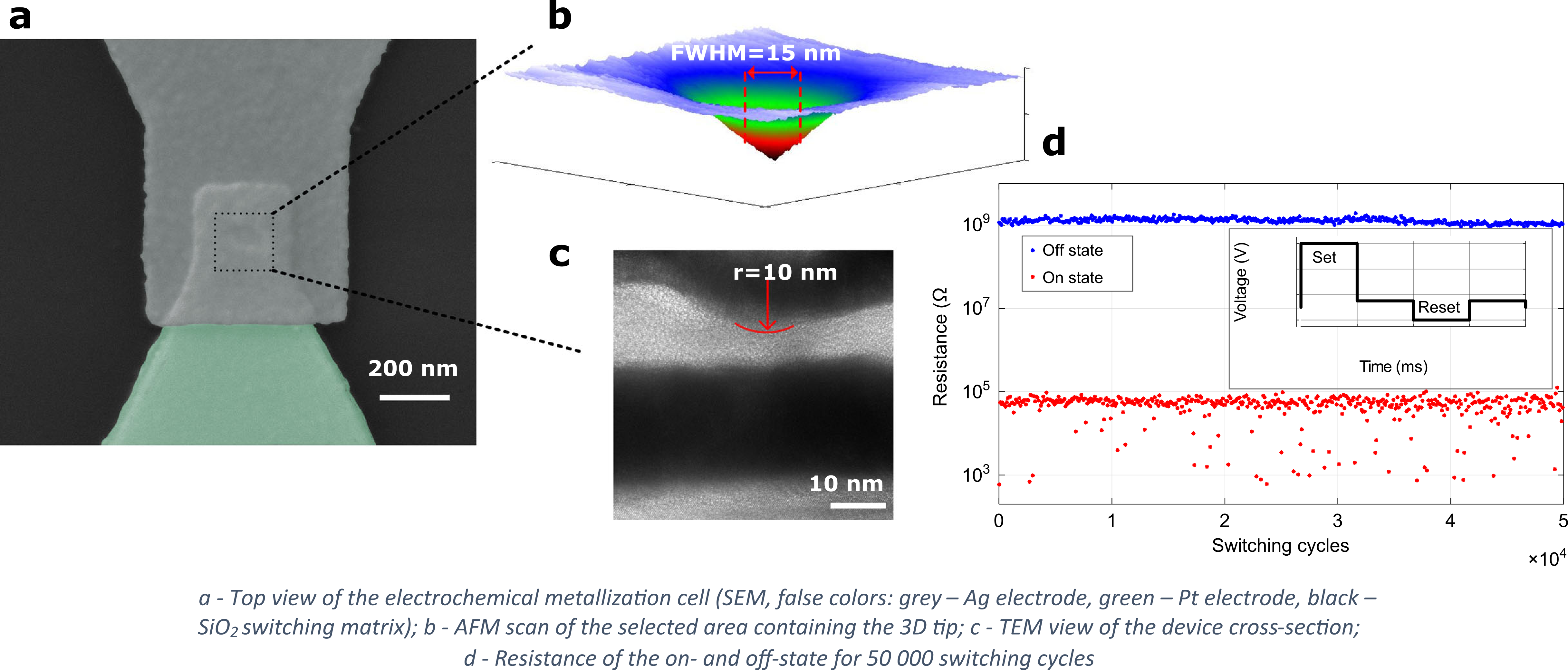
Atomic-scale electrochemical metallization cells enabled by the NanoFrazor were demonstrated by Bojun Cheng and his colleagues from Prof. Leuthold’s group at ETH Zürich. Electrochemical metallization cells (EMC), or conductive bridging random access memory (CBRAM), usually consist of metal-insulator-metal layer stacks, where one metallic player plays a role of an active electrode, and the other – of the inert one. To switch between different states, the cell electrochemically grows or dissolves a tiny metal filament between the electrodes. EMCs reported in Communications Physics feature low switching voltage around 100 mV, operation speed in the nanosecond range, extinction resistance ratio as high as 6 × 10⁵, reliable operations, and the possibility to achieve multi-level behavior.

Such impressive performance at the atomic scale is achieved due to the device geometry: one of the electrodes (Pt) is flat, whereas the other one (Ag) is essentially a 3D tip about 10 nm in radius, creating a highly confined electric field in a few nm-thick SiO2 switching matrix. The tip geometry was defined in the PPA resist using the NanoFrazor and then transferred into the SiO2 by reactive ion etching. During switching, a few-atoms long filament forms between the electrodes, acting as a conductive bridge. In such EMCs, filaments suffer little from Joule heating, as they operates near the ballistic limit and most of the power dissipation occurs in the metallic electrodes and not the filament itself.

Reliable performance together with nm-scale footprint make such EMCs very promising for non-volatile memory applications. With help of thermal scanning probe technology, fabrication of such devices can be significantly scaled up without compromising the dimensions of 3D tip.

Purdue, imec, Indiana announce partnership
Resilinc partners with SEMI on supply chain resilience
NIO and NXP collaborate on 4D imaging radar deployment
Panasonic Industry digitally transforms with Blue Yonder
Global semiconductor sales decrease 8.7%
MIT engineers “grow” atomically thin transistors on top of computer chips
Keysight joins TSMC Open Innovation Platform 3DFabric Alliance
Leti Innovation Days to explore microelectronics’ transformational role
Quantum expansion
indie launches 'breakthrough' 120 GHz radar transceiver
Wafer fab equipment - facing uncertain times?
Renesas expands focus on India
Neuralink selects Takano Wafer Particle Measurement System
Micron reveals committee members
Avoiding unscheduled downtime in with Preventive Vacuum Service
NFC chip market size to surpass US$ 7.6 billion
Fujifilm breaks ground on new €30 million European expansion
Fraunhofer IIS/EAS selects Achronix embedded FPGAs
Siemens announces certifications for TSMC’s latest processes
EU Chips Act triggers further €7.4bn investment
ASE recognised for excellence by Texas Instruments
Atomera signs license agreement with STMicroelectronics
Gartner forecasts worldwide semiconductor revenue to decline 11% in 2023
CHIPS for America outlines vision for the National Semiconductor Technology Center
TSMC showcases new technology developments
Alphawave Semi showcases 3nm connectivity solutions
Greene Tweed to open new facility in Korea
Infineon enables next-generation automotive E/E architectures
Global AFM market to reach $861.5 million
Cepton expands proprietary chipset
Semtech adds two industry veterans to board of directors
Specialty gas expansion
×
Search the news archive

To close this popup you can press escape or click the close icon.
Logo
×
Logo
×
Register - Step 1

You may choose to subscribe to the Silicon Semiconductor Magazine, the Silicon Semiconductor Newsletter, or both. You may also request additional information if required, before submitting your application.


Please subscribe me to:


You chose the industry type of "Other"

Please enter the industry that you work in: