
Entegris CTO outlines key requirements for realizing the promise of Industry 4.0
Silicon Semiconductor technical editor Mark Andrews recently spoke with Entegris CTO, Dr. James O’Neill, about the expanding role that advanced materials and defect elimination are playing as enablers of Industry 4.0, the ‘Fourth Industrial Revolution.’
Q: How are advanced materials responsible for driving the next wave of digital disruption?
A: Over the last five years, we’ve seen an emergence of new technological developments in artificial intelligence, virtual reality, robotics, autonomous vehicles and the Internet of Things (IoT), referred to as “The Fourth Industrial Revolution.”
As described by Klaus Schwab, founder of the World Economic Forum, this new era of computing is the “fusion of technologies blurring the lines between the physical, digital, and biological.”
For example, automakers are using mixed reality technology to aid in the design process when making a new vehicle. Manufacturers can now take a physical product and overlay new virtual concepts onto it during design, speeding up the step between design and build, while also delivering an end product the customer wants.
AI has already started revolutionizing healthcare by leveraging big data analysis to optimize healthcare services. A good example of this is IBM Watson’s ability to analyze a patient’s data and provide personalized treatment plans that combine the patient’s medical history, clinical expertise, external research and data. Identifying patterns in huge data sets of genetic information and medical records by looking for mutations and linkages in diseases will play a key role in addressing chronic disease.
Since so many of these newer applications are dependent on the collection and processing of large amounts of data, there’s market demand for faster processors, more memory, and greater performance of ICs to power the Fourth Industrial Revolution. According to an IDC study, the volume of global data in this era of digital transformation is set to increase 10x to 163 zettabytes (one trillion gigabytes) from 2016 to 2025. And it’s this data storage, analysis, and process that will play a central role in the technology infrastructure; again driving the growth of memory (both DRAM and 3D-NAND), processors (CPU, GPU, FPGA, etc.), and other IC devices, mostly in the leading-edge nodes -- dependent on advanced semiconductor materials.
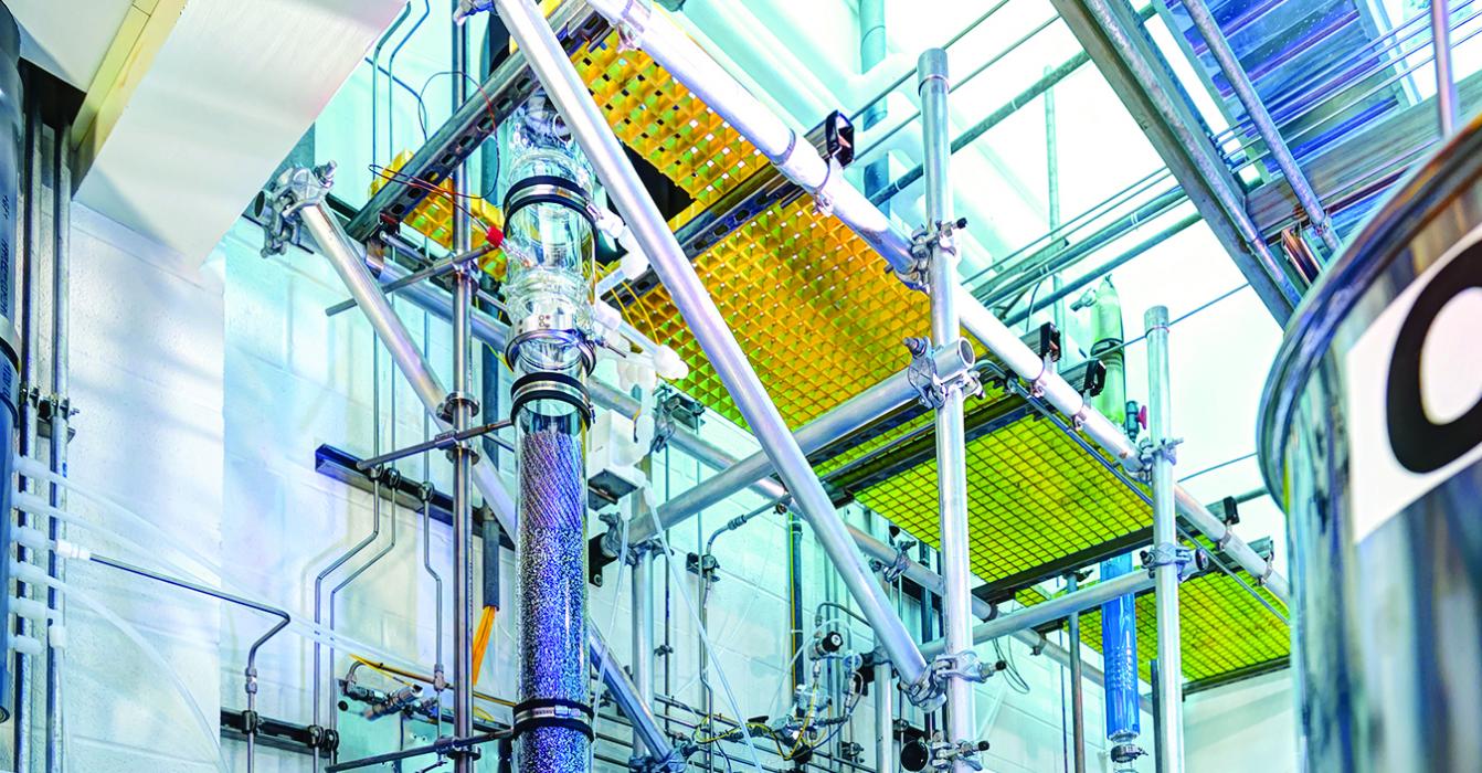
At the heart of these transformations is advanced materials science – the ability to engineer new materials at nanometer scale dimensions. Raw materials like Hf (Hafnium), cobalt, ruthenium, molybdenum, GaN, and graphene are finding their way into integrated chip (IC) manufacturing, and advanced filtration and purification capabilities are required to ensure the integrity of these materials during the manufacturing of the chips. More raw materials will be needed, especially wafers, but also etch gases, precursors, photoresists, and CMP consumables to keep up with the pace of high demand for both leading edge and legacy node chips. We’re already starting to see these new materials being applied. One of the large manufacturers in Taiwan is using advanced resists and extreme ultraviolet lithography (EUV) as a means to pack more electronic circuitry onto a chip, and new interconnect metallurgy to speed the transmission of data from one transistor to another.
With their unique properties and extended application to various industries, advanced materials are driving digital disruption forward. And the new fab processes and purification that is required in the development of semiconductors to power this next wave of technology is critical to long term success.
Q: With all the possibilities offered by cutting edge technologies such as artificial intelligence, robotics, autonomous vehicles, and IoT what’s needed for manufacturers to keep up with the demands for new applications?
A: With all of the new applications of the Fourth Industrial Revolution comes new challenges for which the industry, especially manufacturers, need to prepare. Between the device, the edge and the data center, significant innovation is needed to keep pace with the advancing application space.
For years, the semiconductor industry has been packing big processing power into increasingly smaller chips (aka Moore’s Law). As the traditional scaling approach to Moore’s Law has slowed (it’s more and more difficult to miniaturize a device), there has been pressure to find new ways to improve performance and manage costs through innovations in design, equipment, and materials.
This digital transformation is driving the pressure for faster processors, more memory, and greater performance needs. These pressures are establishing the need for more advanced materials and new device structures (i.e., Fin Field-effect [FinFET] and Gate All-Around [GAA] transistors) at mainstream and leading-edge logic nodes as well as for the development of advanced memory technologies.
For example, new metallurgies like cobalt, ruthenium and molybdenum are being explored to improve the resistivity and reliability of interconnect wiring, and new channel materials are being developed to increase electron mobility and transistor speed. These new materials and the more sophisticated integration flows required to achieve higher performance devices for innovations of the Fourth Industrial Revolution also add multiple fabrication steps and increase process complexity.
To address these challenges, manufacturers need to adopt new processes to work with new materials at scale, increase yields, and reduce contamination risk. Better contamination control and defect reduction will become a bigger focus for manufacturers and a necessary standard, especially when it comes to state-of-the-art applications such as medical devices and self-driving cars. Long-term reliability improvement is not only a social responsibility, but a competitive differentiator as mission critical applications continue to take off.
Q: For years the semiconductor industry has been hinged on Moore’s Law, shrinking chip features to pack more transistors into a smaller area. How has this changed and what are the most important things for manufacturers to consider in light of this change?
A: Until recently, the semiconductor industry has kept to Moore’s Law by “shrinking” chip features to pack more transistors into a smaller area. As the traditional scaling approach to Moore’s Law has slowed (it’s more and more difficult to miniaturize a device), there has been pressure to find new ways to improve performance and manage costs through innovations in design, equipment, and materials while also avoiding chip failure. These are some of the biggest challenges for manufacturers, yet it is required for them to survive and capitalize on the Fourth Industrial Revolution.
To outline further, the key factors for semi manufacturers to consider in this new era include:
Capacity: To handle rapidly increasing volumes of data, more chips are required— both advanced logic and mainstream nodes. While many fabs can incrementally increase output through improved tool performance and yield, there is also the need to build new capacity in every segment. The market for memory is booming but demand will likely continue to outpace planned capacity for both DRAM and NAND in the next few years. The same holds true for sensors and logic. And the capacity challenge isn’t confined to the chip makers. Manufacturing a greater number of more sophisticated chips requires new and more precise equipment.
To address the need for more raw materials, especially wafers, but also etch gases, precursors, photoresists, Entegris recently expanded its Kulim manufacturing capacity and capabilities to add new tooling, molding machines, and numerous updates to the assembly area. This expansion helps Entegris meet the demand for wafer handling products.
Cost: Adding capacity is costly, and so is the innovation needed to improve device performance. For mainstream nodes, new solutions are needed that drive even greater efficiencies in the ongoing effort to reduce costs. On the leading edge, pushing the limits of Moore’s Law requires innovation at every step in the supply chain. As manufacturing processes become more complex, no single company will be able to provide solutions at every step. That means there must be a commitment to collaboration and a more concerted effort as an industry to solve these problems together.
Performance & Complexity: The new materials and more sophisticated integration flows required to achieve higher performance devices add fabrication steps and increase process complexity. Greater complexity, in turn, makes yield ramps more challenging. Process maturity for an advanced node FinFET device is much less than that for a planar device of an earlier node generation. While many industries have to do more with less, the semiconductor industry must do more with more — at least when it comes to complex manufacturing processes. Every new step added to the manufacturing processes creates a potential point of failure and solving each of these challenges is time-consuming and costly.
As the semiconductor industry begins ramping EUV lithography for the high-volume manufacturing (HVM) of advanced technology nodes, keeping EUV reticles defect-free is more demanding than ever. Developed in close collaboration with ASML, Entegris’ revolutionary EUV 1010 Reticle Pod enables customers to safely transition to smaller and smaller line widths, as needed for the most advanced lithography processes. To achieve these levels of performance within the NXE:3400B scanner, Entegris developed new technologies for contacting the reticles and controlling the environment, enabling customers implementing HVM for advanced technology nodes to focus on increasing efficiency and throughput.
Yield & Reliability: To address the challenges of increased process complexity, manufacturers must continue to adopt new processes and materials to enable scaling, better contamination control, and defect reduction to improve yield. Historically, cost and yield have been prioritized above all else. With emerging technologies and applications of the Fourth Industrial Revolution, including medical devices, self-driving cars, and many industrial/infrastructure IoT applications, reliability has become equally if not more important. Long-term reliability improvement is not only a social responsibility but a competitive differentiator, especially for mission-critical devices as these developments continue.
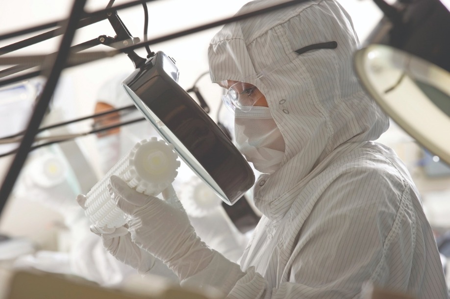
Manufacturers are producing Systems-on-chip (SoCs) at the 7 nm node and soon enough at 5 nm. At this size, any particle or contaminant can make a chip fail; therefore, it’s critical that proper purification is included in the fab process. Entegris works with automakers and mainstream fabs to investigate reducing some of the contaminants and particles that are not affecting yield, yet are causing critical problems in long-term chip reliability. Many existing and mainstream fabs may be yielding 99%- 100%, yet there are undetected defects and imperfections that will still cause reliability issues down the road. This has triggered Entegris to become an industry advocate on a new effort to reduce contaminants, considering the greater risk of mission-critical and consumer facing apps (self-driving cars) that are being developed today.
Q: Why it is so important for these chips to be contaminant-free?
A: With the Fourth Industrial Revolution comes an increased recognition of the importance of advanced materials science, not only to create high performance, pure materials used in the fabrication of advanced chips, but also to ensure their integrity from the point where they are manufactured until they are consumed on the chip. This means purity matters like never before, with even smaller defects leading to yield loss as the dimensions of advanced devices shrink below 10 nm. While the primary focus of defect learning has historically been on killer defects that affect initial chip yield, increasing focus is now being placed on eliminating smaller defects that influence long-term reliability. Eliminating such “latent” defects, increasing the result of undetected contaminants and pattern imperfections, are ever more important in applications such as autonomous vehicles where long-term reliability is critical.
To outline this scenario further, the average car has between 30 to 50 computer chips, and luxury cars may have as many as 100 of these microprocessor-controlled devices, known as electronic control units. A fully autonomous car, however, which needs high performance chips to send processed data feeds into a central computer which then decides whether the car should brake, slow down, accelerate, etc, could have up to 10,000 ICs. If any component in an autonomous car system fails, the car may not collect crucial data it needs to execute on its next step, the possibility for failure is multiplied. With this many chips in each car, if you have a failure rate of one chip out of 1 million, then several hundred cars might fail on the roads every single day. The resulting repairs, medical bills, and lawsuits would be costlier than fixing the reliability issue at the outset.
Of greater concern are chips that have passed through the fab production line as 100% yield but can still fail in the field. The design process for Fourth Industrial Revolution technologies such as automotive applications must be accompanied by very high awareness of the reliability consequences. Entegris is providing solutions to eliminate some of the random inferences impacting reliability.
Q: How are leading manufacturers addressing the issue of more rigorous testing requirements mandated by more sophisticated chip manufacturing?
A: As semiconductor manufacturers move to advanced nodes required for critical applications in artificial intelligence, autonomous driving, blockchain, IoT, etc., it’s critical that material supplier partners continuously enhance their local development capabilities. With continued investment in its Taiwan Technology Center and state-of-the-art clean manufacturing facility in Kulim, Malaysia and local manufacturing, Entegris is poised to meet demands in critical yield, reliability and performance customers face today and tomorrow.
With the introduction of the SP3 wafer inspection tool at its Taiwan Technology Center last year, Entegris has expanded its local wafer inspection capability down to 19nm. This new addition and related infrastructure including Class 10 Clean Room and an ACT12 coater, together with the knowledgeable and seasoned team of scientists at the Taiwan Technology Center, enables Entegris to generate its own on-wafer defect data to guide new product development and improve product performance.
Q: As with previous industrial revolutions, the development of semiconductor materials and gases required to fuel the demands of today’s technology creates environmental concerns. How can manufacturers address these concerns?
A: As we continue to see a rapid increase in advanced technologies of the Fourth Industrial Revolution, we will also see a stronger focus on green manufacturing and improved efficiencies to meet regulatory demands. Leading semi manufacturers are starting to lay the foundation for sustainable manufacturing processes and flexible logistical solutions for the transportation and disposal of toxic chemicals in an effort to lower their carbon footprint.
Q: As disruptive innovations in IoT, AI, ML and analytics become more and more central to business and consumer technologies and everyday life, what additional advancements in materials are needed to generate these applications?
A: The Fourth Industrial Revolution is transforming the semiconductor industry as we know it, creating a market dependent on a diverse array of high-performance chips to power IoT, AI, AR/VR and more. As stated above, the proliferation of these applications and devices is poised to drive unprecedented levels of demand for memory, processing speed, and bandwidth. The semiconductor industry must evolve to serve this rapidly growing market opportunity.
Rather than addressing challenges step-by-step and vendor-by-vendor, industry collaboration from across the supply chain is needed to identify potential challenges and solutions. That means IDMs, foundries, OSATs, equipment, materials, and component companies will need to work together to meet capacity, cost, performance, yield and reliability challenges.
Improvements in product design, manufacturing, and contamination control are also needed, and by working together, higher standards can be achieved as well as lower costs and greater efficiencies. A reduction in — or even the elimination of — friction points along the way, with contamination control for risk mitigation as one of the highest priorities, will be key to addressing the vast opportunities presented by this new age of computing.

Dr. James O’Neill is Chief Technology Officer of Entegris where he leads global development efforts in new material solutions for the industry’s most challenging issues. With over 23 years of leadership and management experience in semiconductor research, development and manufacturing, O’Neill has held positions at ATMI before it was acquired by Entegris in 2014, and in 14nm technology development at IBM. Dr. O’Neill earned a Ph.D. in Physical Chemistry at Columbia University and a Bachelor’s degree in Chemistry from Yale University.


