
Olympus Stream software. Inspection without limitation
With the new Olympus Stream 2.4 software, users in all industries – from electronics and semiconductors to general manufacturing, steel production and automotive – can now conduct fast and precise observations on a large variety of samples while maintaining data security and measurement reliability.
Simple camera and microscope control makes analysis easy for users who often change their workstations, and intuitive step-by-step workflows enable multiple operators to use the same software for different inspection tasks. All results are centralized in one location. Available in eight languages, Olympus Stream guides operators at every step, from image capture and measurement to sharing of results, reducing the need for training, thereby saving time and cost.
Creating a report often takes longer than the image capture and analysis, so Olympus Stream enables users to produce smart, sophisticated and easily-editable reports. The software includes the most comprehensive range of the latest international materials science standards, so customers can be assured of compliance in their relevant industry and region.
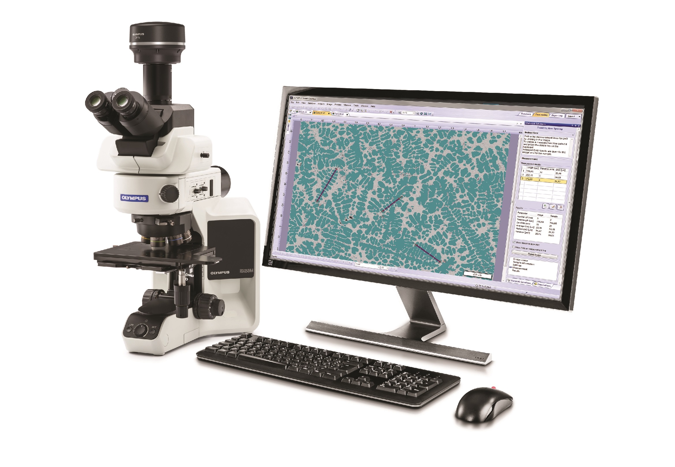
Olympus Stream 2.4 now supports IR imaging for enhanced, non-destructive inspection of silicon wafers and solar cells at the end of the manufacturing process. It also supports various illumination methods, including MIX observation, which enables users to highlight defects and differentiate raised surfaces from depressions that are normally difficult to see with conventional microscopes. For real-time analysis on the production line, the live imaging functionality means users can immediately respond to complex problems, thereby reducing overall analysis time and increasing productivity. The new dendrite arm spacing function automatically measures the mean secondary dendrite arm spacing in lightweight aluminium casting to monitor solidification time, a key factor for improving mechanical properties, such as tensile strength and elongation. Enhanced ability to measure simple and complex porosity means that users can be confident in their weld assembly and additive manufacturing inspections.
When an operator needs to be able to quickly capture a larger, panoramic image, or where they need an extended depth of focus, Olympus Stream has the answers. The Extended Focus Image (EFI) function combines multiple Z-level images to build a single image that is entirely in focus, and Instant Multiple Image Alignment (MIA) enables users to create panoramic images simply by moving the XY stage, without the need for a motorized stage.
The new Olympus Stream 2.4 software is optimized for Olympus hardware, so that all are controlled with the same easy-to-use interface. Featuring many sophisticated updates, Olympus Stream makes it as easy as possible for users to acquire sharp, crisp images for quantitative measurements and reporting based on the latest standards, no matter the application.


