

Plasma Etching – NE-550, NLD-570, NE-5700, NE-7800, NLD-5700
ULVAC offers dry etching systems for MEMS, compound semiconductors, power devices, LED, RF devices, optical films and ceramics. More than 700 system installed are evidence in dry etching knowledge, quality and reliable process results.
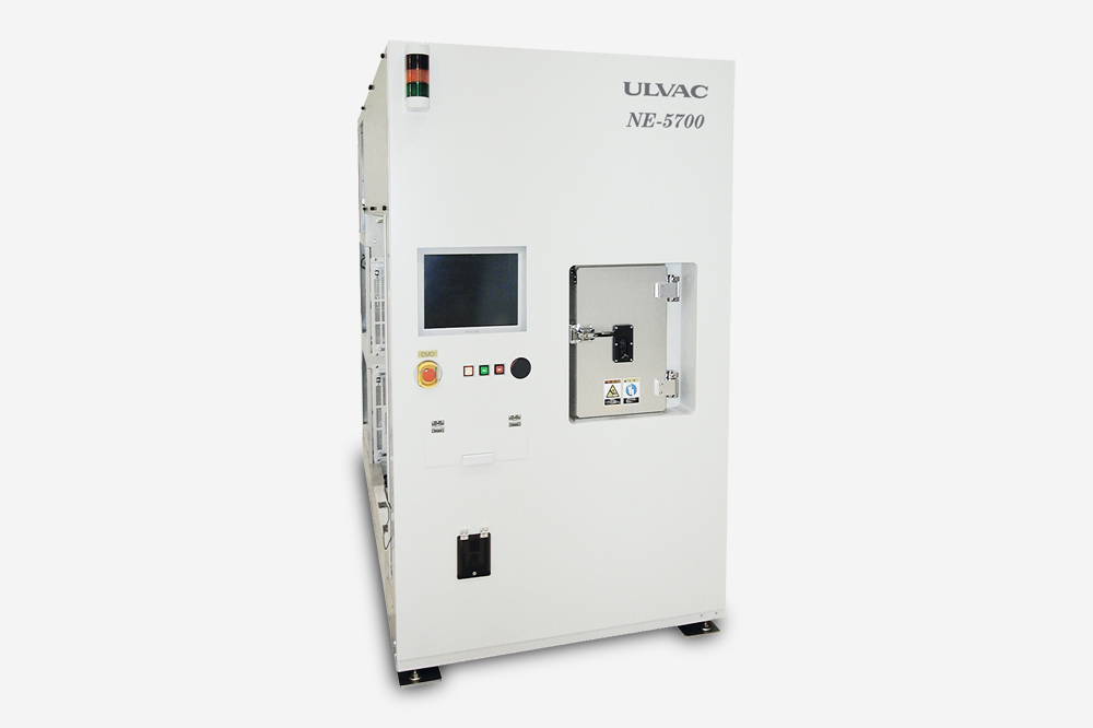
The NE-5700, NE-7800, NLD-5700 etching systems for high volume mass production are available as four core and six core cluster platforms from single chamber up to four chamber system and up to two vacuum cassette chambers including ICP etching and ashing. The NE-550 and NLD-570 etching systems for R&D are equipped with one process chamber and single wafer vacuum load lock or vacuum cassette.
NE series offers the best RIE process in LED, RF Device, SiC, metal (Al, Al alloy, Mo, Ti, Ta, Ru, W, Cr), noble metal (Pt, Ir, Au), III-V Materials (GaN, AlGaN, InP, GaAs, AlGalnP), and Ferro-Electric Materials (PZT-stack, AlScN-stack, STO, BST), ITO, Al2O3, SiC, Diamond. For metal etching a stable etching rate can be achieved using ULVAC`s patented star electrode design.
For none volatile etching components the NE etching chamber is equipped with high temperature control of shields, chamber, gate valve, TMP and piping.
High selective etching between thick ferroelectric layer and thin bottom electrode can be achieved without side wall deposition to avoid deterioration of the electrical properties of ferroelectric capacitors in production. For Al etching the NE-7800R system can be equipped with Al etching chamber, dry ashing chamber and two atmospheric chambers for rinsing and wet resist removal to avoid any post etch corrosion.
NLD series offers the best RIE process for SiO2 trench etching (vertical or taper) for optical MEMS and wave guides; quartz and glass (Pyrex, fused glass, Borsilicat) etching for BIO-MEMS, smooth sidewalls Si-vias etching for packaging and etching of LiNBO3 for SAW.
Both, NE and NLD etching chambers are available for 100~200mm wafer size including perfect wafer temperature control using mechanical clamping or ESC. For the control of the etching uniformity both systems have low pressure operation below 0.1Pa with High Plasma Density of 5E10~1E11/cm-3 @ 0.1Pa Ar-plasma and low electron temperature of 3~5eV.
All systems can be equipped with wafer ID reader and SECS/GEM as option.
All offer low CoO, good maintainability, small footprint, superior process performance with Japanese quality and are locally supported by an extensive European operation. Located near Munich, our team of experienced engineers and sales people ensure a fast and professional response to customer requests. Request a free demo today.
https://www.ulvac.eu/en/products/equipment/by-technology.html


