
Applied Materials Enables Emerging Memories for the IoT and Cloud Computing
Applied Materials, has unveiled innovative, high-volume manufacturing solutions aimed at accelerating industry adoption of new memory technologies targeting the Internet of Things (IoT) and cloud computing.
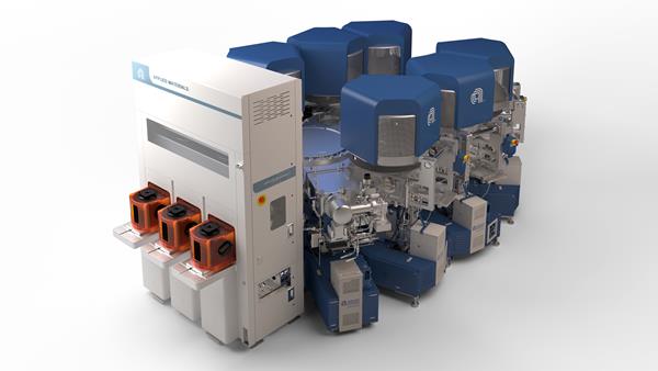
Applied Materials’ new Endura Clover MRAM PVD platform is made up of nine unique wafer processing chambers all integrated in pristine, high-vacuum conditions. It is the industry’s first 300-millimeter MRAM system for high-volume manufacturing capable of individually depositing up to five different materials per chamber.
Applied Materials' Endura Impulse PVD platform for PCRAM and ReRAM includes up to nine process chambers integrated under vacuum along with on-board metrology to allow the precise deposition and control of the multi-component materials used in these emerging memories.
Today’s high-volume memory technologies including DRAM, SRAM and flash were invented decades ago and have become ubiquitous in digital devices and systems. New memories – notably MRAM, ReRAM and PCRAM – promise unique benefits, but they are based on new materials that have been too challenging for high-volume manufacturing. Today, Applied Materials is introducing new manufacturing systems that allow novel materials – the key to these new memories – to be deposited with atomic-level precision. The company is delivering the most advanced systems it has ever developed to enable these promising new memories to be reliably produced at an industrial scale.
“The new Endura platforms we are introducing today are the most sophisticated chip-making systems our company has ever created,” said Dr. Prabu Raja, senior vice president and general manager of Applied’s Semiconductor Products Group. “Our broad portfolio gives us the unique ability to integrate multiple materials engineering technologies along with on-board metrology to create new films and structures that were not possible until now. These integrated platforms illustrate the critical role that new materials and 3D architectures can play in giving the computing industry entirely new ways to improve performance, power and cost.”
“IBM has been spearheading R&D of new memories for many years, and we see the need for these technologies increasing as the AI era demands improvements in chip performance and efficiency,” said Mukesh Khare, vice president, Semiconductors, AI Hardware and Systems, IBM Research. “New materials and device types can play an important role in enabling high-performance, low-power embedded memory for IoT, Cloud and AI products. Applied Materials’ high-volume manufacturing solutions can help accelerate the availability of these new memories across the industry.”
“Improving the efficiency of data centers is a key priority for cloud service provider and enterprise customers,” said Sung Gon Jin of SK hynix, head of the Advanced Technology Thin Film Group. “In addition to providing continued innovations in DRAM and NAND, SK hynix is pioneering the development of next-generation memories that can help boost performance and reduce power consumption. We value the work of Applied Materials in collaborating with us to speed the development of new materials and high-volume production techniques for promising emerging memories.”
“As advancements in AI, machine learning and IoT drive workloads to become increasingly data-intensive and complex, new innovations in memory technology will be needed to effectively process them,” said Richard New, vice president of research, Western Digital. “Applied Materials is providing important technology to help accelerate the availability of promising emerging memories such as MRAM, ReRAM and PCRAM.”
MRAM for the IoT
The computer industry is building the Internet of Things whereby sensors, computing and communications are incorporated into tens of billions of devices that will monitor their environments, make decisions and send critical information to cloud data centers. MRAM (magnetic random access memory) is a leading candidate to be the memory of choice for storing IoT device software and AI algorithms.
MRAM incorporates delicate magnetic materials commonly found in hard disk drives. MRAM is inherently fast and also nonvolatile, allowing software and data to be retained even when power is removed. Due to its fast performance and high endurance, MRAM may eventually be used as an alternative to SRAM in level 3 cache memory. MRAM can be incorporated into the back-end interconnect layers of IoT chip designs, thereby enabling smaller die sizes and lower costs.
Applied’s new Endura Clover MRAM PVD platform is made up of nine unique wafer processing chambers all integrated in pristine, high-vacuum conditions. It is the industry’s first 300-millimeter MRAM system for high-volume manufacturing capable of individually depositing up to five different materials per chamber. MRAM memories require precise deposition of at least 30 different layers of material, some of which are 500,000 times thinner than a human hair. Process variations of just a fraction of the diameter of an atom can greatly affect device performance and reliability. The Clover MRAM PVD platform includes on-board metrology that measures and monitors thickness of the MRAM layers with sub-angstrom sensitivity as they are created, to ensure atomic-level uniformity without risking exposure to the outside environment.
“As an extremely fast, high-endurance nonvolatile memory, MRAM is poised to displace embedded flash and level 3 cache SRAM in both IoT and AI applications,” said Tom Sparkman, CEO of Spin Memory. “The availability of a high-volume manufacturing system from Applied Materials is a huge boost to the ecosystem, and we are thrilled to be working with Applied to deliver MRAM solutions and accelerate its adoption.”
ReRAM and PCRAM in the Cloud
As data generation grows exponentially, cloud data centers require order-of-magnitude improvements in the speed and power consumption of the data pathways linking servers and storage systems. ReRAM (resistive RAM) and PCRAM (phase change RAM) are fast, nonvolatile, low-power, high-density memories that can be used as “storage class memory” to fill the widening price-performance gap between server DRAM and storage.
ReRAM is made using new materials that act like a fuse, allowing filaments to be selectively formed within the billions of storage cells to represent data. In contrast, PCRAM incorporates the phase change material found in DVD disks, and bits are programmed by changing the state of the material from amorphous to crystalline. Similar to 3D NAND memories, ReRAM and PCRAM are arranged in 3D structures, and memory makers can steadily reduce the cost of storage by adding more layers with each product generation. ReRAM and PCRAM also offer the possibility of intermediate stages of programming and resistivity to allow multiple bits of data to be stored in each memory cell.
ReRAM and PCRAM both promise significantly lower cost than DRAM along with substantially faster read performance than NAND and hard disk drives. ReRAM is also a leading candidate for future in-memory computing architectures whereby computing elements are integrated into the memory arrays to help overcome the data movement bottleneck associated with AI computing.
Applied’s Endura Impulse PVD platform for PCRAM and ReRAM includes up to nine process chambers integrated under vacuum along with on-board metrology to allow the precise deposition and control of the multi-component materials used in these emerging memories.
“Uniform deposition of the new materials used in ReRAM memories is critical to achieving the highest possible device performance, reliability and endurance,” said George Minassian, CEO and co-founder of Crossbar, Inc. “We specify the Applied Materials Endura Impulse PVD system with on-board metrology in our ReRAM technology engagements with memory and logic customers because it enables a breakthrough in these critical metrics.”


