
Photonic technologies are converging into a CMOS compatible silicon photonic platform
Silicon photonics technology has definitely reached a first level of maturity, as it can be found nowadays in commercial products for intra- and inter-datacenters communications at high data rates. Higher volume markets such as intra-rack communications could be addressed by solving three main challenges: the packaging, the energy consumption, and the laser integration.
By Karim HASSAN, PhD, Researcher and Project Manager at CEA-Leti
The convergence of photonic technologies into a CMOS compatible silicon photonic platform remains a key challenge while several fabrication supply chains and industrial products are available in the field of high speed communications on optical fiber. Nowadays, the circuit design tools are available on several software platforms. However, silicon photonics is still suffering from the lack of integrated light sources. Existing packaging solutions offer a straightforward way to combine III-V laser sources and silicon photonics integrated circuits in order to address the market today, at the expense of a high cost and low volume production. On the other hand, the hybridization of III-V gain material (which remains the materials of choice to achieve semiconductor laser sources) can be realized using III-V direct bonding on top of patterned silicon. Subsequent laser demonstrations relying on CMOS-compatible process for the silicon part have been in most cases followed by process steps carried out with small wafer III-V fabrication lines (typically below 4-inch wafers). With such integrations, the cost advantage of silicon photonics based on the use of CMOS platforms and large wafer format is not valid.
The issues regarding the integration of III-V material go beyond the introduction of the material itself on CMOS lines. In fact, fundamental aspects such as having a low access resistance with CMOS back-end of line (BEOL) metals onto III-V compounds is not straightforward since noble metals, e.g. gold, cannot be used. The thin SOI (<310 nm) used for getting single mode silicon photonic integrated circuits (PICs) makes optical coupling with the thick III-V gain material (>2µm) difficult. It is worth noting that the topology of III-V components, having a large height of about 3mm, makes the co-integration within the BEOL of active silicon devices interconnects incompatible.
Furthermore, while large format of III-V wafer epitaxy is still in progress, most of the III-V suppliers can provide laser stack onto wafers smaller than 4 inch, which makes the use of dies rather than wafer mandatory for the hybridization on 200 mm silicon wafer (as well as 300 mm).
Nevertheless, the use of III-V dies generates additional difficulties for III-V processing due to undesired lateral etching of the dies during the III-V substrate removal. An overall integration strategy must be developed in order to solve these technological barriers.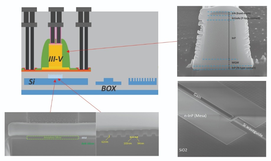
Figure 1. Schematic view and scanning electron microscopy images of III-V on silicon laser fabricated on 200 mm CMOS lines.
Successful laser integration on fully CMOS-compatible silicon photonics platform
In order to break the existing technological limitations for mass production of hybrid PICs, CEA-Leti’s R&D fabrication platform has developed a first laser integration on a 200 mm fully CMOS-compatible silicon photonics platform, as depicted in the Figure 1.
The fabrication process can be divided into three main parts, with first the silicon patterning followed by the III-V hybridization through molecular bonding, prior to the III-V patterning (including the CMOS metallizations). The optical coupling between III-V and silicon requires thick silicon waveguides, which is obtained by a localized thickening with amorphous silicon, as shown in Figure 1. Next, a chemical and mechanical planarization (CMP) is used to provide a smooth oxide layer for the direct bonding of III-V on silicon. The novel patterning of the III-V material that has been developed relies entirely on the 200 mm platform. The new process flow proposed by CEA-Leti uses selective reactive ion etching (RIE) steps on both p-InP and p-InGaAsP.
New BEOL for lasers
Such a new patterning sequence allows us to encapsulate the III-V completely prior to the BEOL, which will remain planar, similar to standard silicon photonics components. Consequently, a high density of vias can be patterned on the SiO2 encapsulation and subsequently filled with tungsten on top of both contact sides made of Ti metallization deposited by magnetron sputtering (PVD), prior to the final AlCu micron-thick pad layer, as depicted in Figure 2.
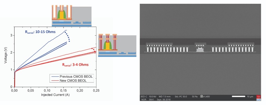
Figure 2. Experimental IV curves on 200mm CMOS hybrid lasers with 1 and 2 levels of BEOL and scanning electron microscope view of the cross-section of such laser developed on CEA-Leti’s R&D fabrication platform.
This new CMOS BEOL for lasers, developed within the framework of the IRT Nanoelec Photonic Program, a French consortium involving CEA-Leti, ST Microelectronics, ALMAE, CNRS-LTM, and Mentor Graphics, results in a state-of-the-art serial resistance on hybrid lasers ranging from 3 Ohms to 4 Ohms.
Large scale automated testing
Large scale automated testing is also of great interest when arguing about large volume production of hybrid PICs. Thanks to the novel 200 mm process, full wafers can be thoroughly mapped with electro-optical fiber-to-fiber measurements. Such a test is made possible by the use of fiber grating couplers fabricated onto the silicon, similarly to standard silicon PICs. Most of the developments required specifically for the tests of hybrid lasers relies on the spectral (CW and pulsed) and thermal characteristics. Even though silicon devices are also sensitive to temperature variations, the behavior of hybrid lasers regarding thermal fluctuation and the aging of such object is vital to ensure the operability on datacenter environments.
There are still some challenges in this regard to provide high temperature tests before the packaging, with, for instance, the improvement of optical fiber position and vibrations due to convection over the wafer and dilation of it. The development of on-wafer laser testing is not only relevant for the monitoring of the fabrication yield, but also for sorting out the hybrid photonics chips as a function of their performances before packaging.
Efficient die bonding
Beyond the performances and efficiency, the cost of hybrid III-V/Si transceivers is of great interest. While mass production of silicon chips is cheap, the addition of III-V materials can increase significantly the budget per PIC. One can note that the consumption of III-V material must be minimized in order to reduce the environmental impact (by the material itself or the chemicals used for waste treatment). Figure 3 shows 3 mm x 3 mm III-V dies on top of a 200 mm SOI wafer (including silicon photonics circuits for high lasers) after the molecular bonding. The newly developed 200 mm die bonding reached a yield ranging from 70 to 99%, with 90% of the successfully die transferred having 99% of III-V material bonded onto the SOI surface. While the molecular bonding itself can be executed the same way as wafer bonding, the substrate removal is more critical for dies due to undesired lateral etching.
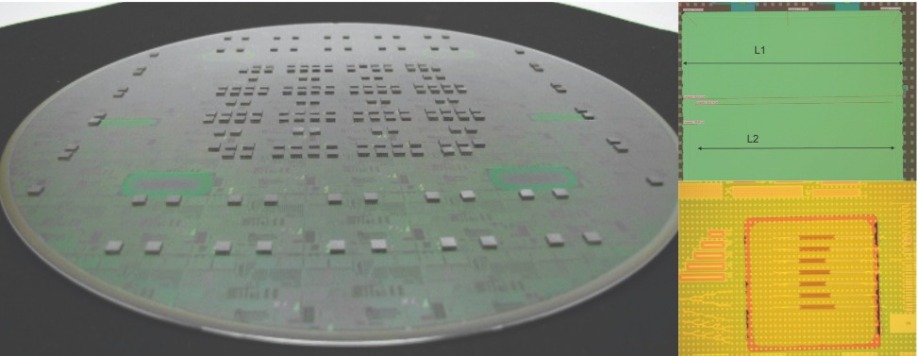
Figure 3. III-V dies on 200 mm silicon wafer, and microscope images of such die after the III-V substrate removal and during the 200 mm CMOS process of hybrid lasers.
The thinning was ensured by first an original sequence of grinding operation down to 50 mm III-V remaining prior to a chemical wet etching used to remove the remaining part of the substrate. By adding a grinding step before the wet etching, the lateral consumption of III-V during the substrate removal was reduced by a factor between 3 and 5. The III-V patterning on those dies is now in progress to realize hybrid lasers.
Conclusions
Recent developments led by CEA-Leti within IRT Nanoelec have led to a full CMOS friendly laser integration process, exhibiting very low serial resistance thanks to novel contacts metallurgy. In addition, wafer scale approaches allows high yield bonding of reduced area III-V coupons/dies onto SOI wafers, drastically reducing the cost of next generation photonic transmitters. The scalability towards 300 mm for both CMOS contacts and die bonding is currently under development, paving the way for the adoption of silicon photonic technology in a variety of emerging applications such as system in a package photonic transceivers, high performance computing and PIC based LiDARs.


