
memsstar Ships MEMS Production System to University of Freiburg
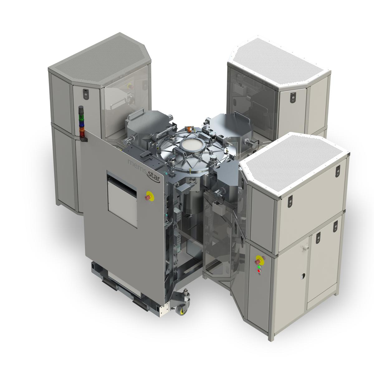
memsstar, a provider of etch and deposition equipment to manufacturers of semiconductors and microelectrical mechanical systems (MEMS), has announced shipment of its three-chamber ORBIS 3000 system for MEMS research and manufacturing to the Department of Microsystems Engineering (IMTEK) at the University of Freiburg, Germany. As part of the nationally funded project, “Processes and Materials for More-than-Moore Electronic Systems (PROMYS),” memsstar’s surface micromachining cluster tool will serve as a central unit for the micromechanical structuring of MEMS components for up to 200mm wafers.
PROMYS is one of 12 projects funded by the Germany Federal Ministry of Education and Research (BMBF) as part of the ForLab (Microsystems Research Laboratory - Germany) initiative. Its research aims to develop IoT solutions, particularly for the application area of medical aids and biological analytical microsystems. The motivation is to defend against degenerative diseases and to enable anywhere-care solutions, for example. The memsstar ORBIS tool will be a key component in achieving heterointegration of all kinds of micromachined sensors and actuators, together with microelectronics and media access, such as fluidic components.
“This project strongly showcases ORBIS’ capabilities and our approach to working with our customers to develop processes that address their specific requirements,” said Tony McKie, CEO of memsstar. “The work being done at Freiburg is truly leading edge, and requires the advanced control and capabilities of our technology to meet the varied application requirements in production there.”
Prof. Alfons Dehe, holding the endowed Georg H. Endress Professorship for Smart Systems Integration, inspires researchers to co-integrate a range of MEMS and semiconductor technologies into systems in order to greatly reduce their size or enable functions that were not previously possible. This includes materials, nano-sized sensor elements and interconnection solutions merged in a seamless fabrication flow form, e.g., ultra-small environmental sensor systems.
“The ForLab initiative triggers numerous research collaborations between universities, Fraunhofer institutes and Hahn-Schickard,” commented Prof. Dehe, also director of the Hahn-Schickard Institute in Villingen-Schwenningen. “Hence, we bridge fundamental research into applications. We not only transfer results to industry, but bridge the gap of small quantity production to SMEs. The memsstar platform offers unique technologies for advanced process control, with faster process times, denser, more robust films, superior within-wafer uniformity and wafer-to-wafer repeatability.”
Introduced in 2014, memsstar’s ORBIS systems deliver the industry’s most advanced single-wafer process capability for advanced MEMS manufacturing. It includes fully integrated process monitoring and endpoint control, a high-selectivity package and a proven hardware that delivers excellent uniformity and repeatability, critical to improving yield.


