Onto Innovation Announces Multiple Orders for Lithography System

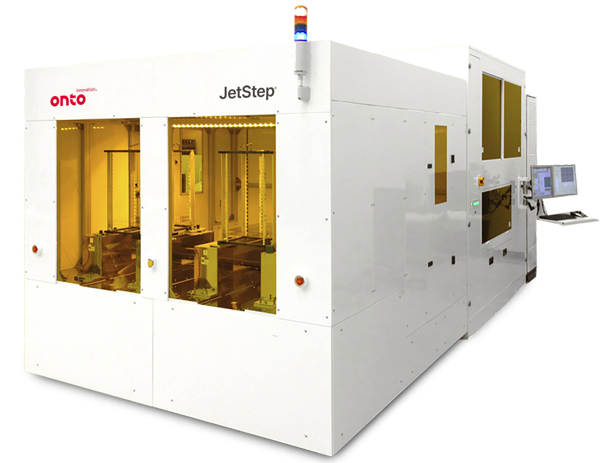
Onto Innovation Inc.announced it has received multiple purchase orders for its JetStep projection lithography stepper from three leading manufacturers. The systems will be utilized for advanced packages using a large panel format to support growth driven by the need to combine various heterogeneous chips into a single package, known in the industry as either chiplets, heterogeneous chip packaging, or system-in-package.
The JetStep lithography solution serves the growing demand for heterogeneous chip packaging coming from the anticipated 5G market that includes smartphones, data centers, AI and IoT applications. The packaging market growth for these applications based on forecasts by TechSearch, Prismark, and internal estimates is currently at 14% CAGR for large format heterogeneous integration from 2019 to 2024.
Including these orders, the lithography backlog is now approximately $15 million. All systems from this current backlog are expected to be delivered in the first half of 2021.
“Next-generation packaging technologies require tighter overlay to accommodate a larger package size with finer pitch chip interconnects on large format flexible panels,” said Alex Chow, vice president of advanced packaging solutions at Onto Innovation. “Heterogeneous integration enables next-generation device performance gains by combining multiple silicon nodes and designs inside one package. The package size is expected to grow significantly, increasing to 75x75mm and 150x150mm, within the next few years. The JetStep lithography system offers a large exposure field size that enables packages well over 250mm2 without the need for image stitching while exceeding aggressive overlay and critical uniformity requirements for these packages.”
Chow added, “The JetStep lithography system is designed to offer production flexibility to meet these new technical challenges and address customers’ technology roadmaps. We believe these system orders from leading-edge manufacturers are a validation of our development efforts. We look forward to working with these valued customers to support their exciting production and technology roadmaps for high-performance computing.”
Kevin Heidrich, senior vice president of marketing concluded, “Onto Innovation is delivering a complete solution to meet the challenges of panel level packaging. A combination of metrology and inspection on our Firefly panel system, with feedforward and feedback control using our Discover software, enables users of the JetStep lithography system to achieve higher productivity and better process control. Our combination of technology is a unique solution that can provide faster production ramps at higher yields for our customers. We continue to collaborate closely with our customers to ensure their success as they migrate to the next generation of advanced packaging technology.”


