
Park Systems Announces NanoScientific Symposium Asia - November 24-25 2020
Park Systems and NanoScientific Publications announce NanoScientific Symposium Asia, which will be held virtually on Nov. 24-25, 2020. The event is for nanoscience researchers and scientists to learn about the latest studies being formed using SPM and is sponsored by Physics World and Nanotechnology World Association.
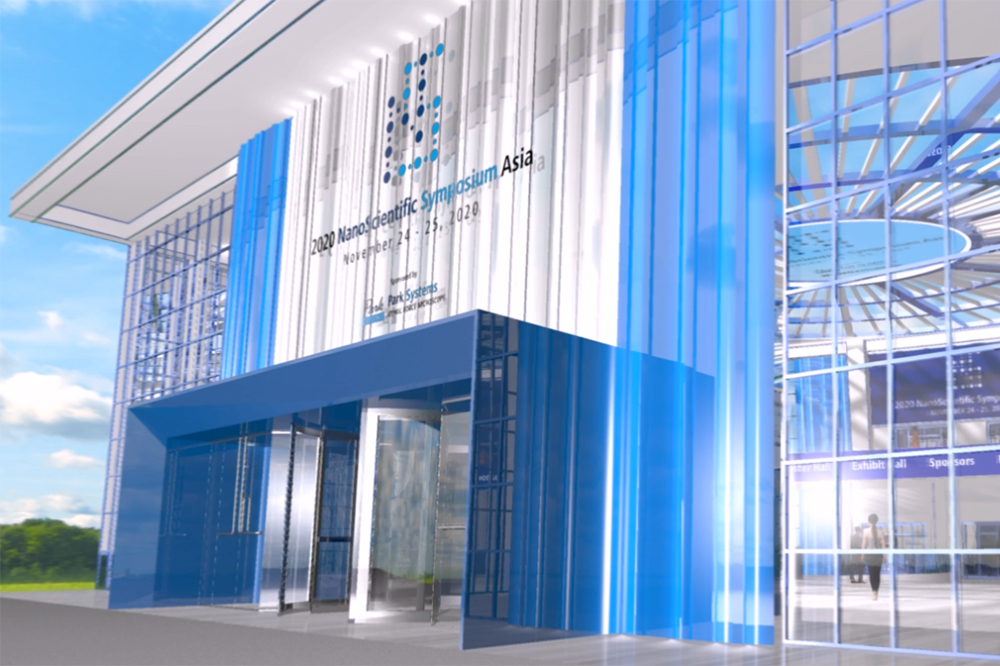
For more information and to register, please go to: https://live.parksystems.com/nssa2020/
“NanoScientific Symposium Asia is a valuable opportunity for people doing scientific research using SPM who want a chance to hear from and network with experts in the field,” states Keibock Lee, Park Systems President. “We encourage all who are interested in Nano Metrology to attend and experience these insightful presentations.”
Scanning probe microscopy, including the AFM, is gaining popularity thanks to its powerful nanoscale imaging and measurement capability, versatility in applications from semiconductor, chemistry to life sciences and recent advances in the ease of use. This virtual event brings together a leading group of experts on a variety of topics and will be a great networking opportunity.
"The Nanotechnology World Association is proud to sponsor the NanoScientific Symposium Asia. It is a great opportunity to hear from academic and industrial experts from across the world, as they share their perspectives and insights on multiple topics relevant to all of us. We invite all professionals in our field to attend," comments Marine Le Bouar, CEO, Nanotechnology World Association, sponsor of NanoScientific Symposiums.
Some of the presentations at NanoScientific Symposium Asia include:
- Prof. Nam-Joon Cho | Nanyang Technological University, Singapore
Nanomechanical Mapping of Viral Protein Binding Interactions with Phosphoinositide Receptors and Pharmaceutical Drug Screening
- Dr. Jae Sung Yun | University of New South Wales, Australia
Probing nanoscale defects in emerging photovoltaic materials using scanning probe microscopy
- Dr. Tan Kim Song | Malaysian Rubber Board, Malaysia
Studies of natural rubber (NR) based materials using atomic force microscopy (AFM) technique.
- Dr. Wang Junyong | National University Singapore, Singapore
Light-emitting diodes based on atomically thin semiconductors
- Dr. Sang-Joon Cho | Park Systems, Korea
Optical Hybrid SPM technology Development
- Dr. Murni Handayani | Indonesian Institute of Sciences, Indonesia
Two wired single molecular diodes based on porphyrin-imide dyads connected covalently between Single-walled carbon nanotubes as electrodes
- Ilka Hermes (Principal Scientist) | Park Systems Europe, Germany
Stabilizing the piezoresponse via dual frequency resonance tracking
- Dr. Persia Ada N. de Yro | Department of Science and Technology, Philippines
Nanomaterials charactization and nanotechnology research in DOST-ITDI
- Dr. Jake Kim | Park Systems, Korea
A comparative study for surface potential mapping using KPFM
NanoScientific published quarterly since 2014 showcases advancements in the field of nanoscience and nanotechnology across a wide range of multi-disciplinary areas of research and has a global distribution of over 40,000 in North America, Europe and Asia. NanoScientific Symposiums in 2019 are also being held in New York, Italy, Korea, China & Mexico.


