
TESCAN New Delayering Capability for Unattended, Automated Failure Analysis
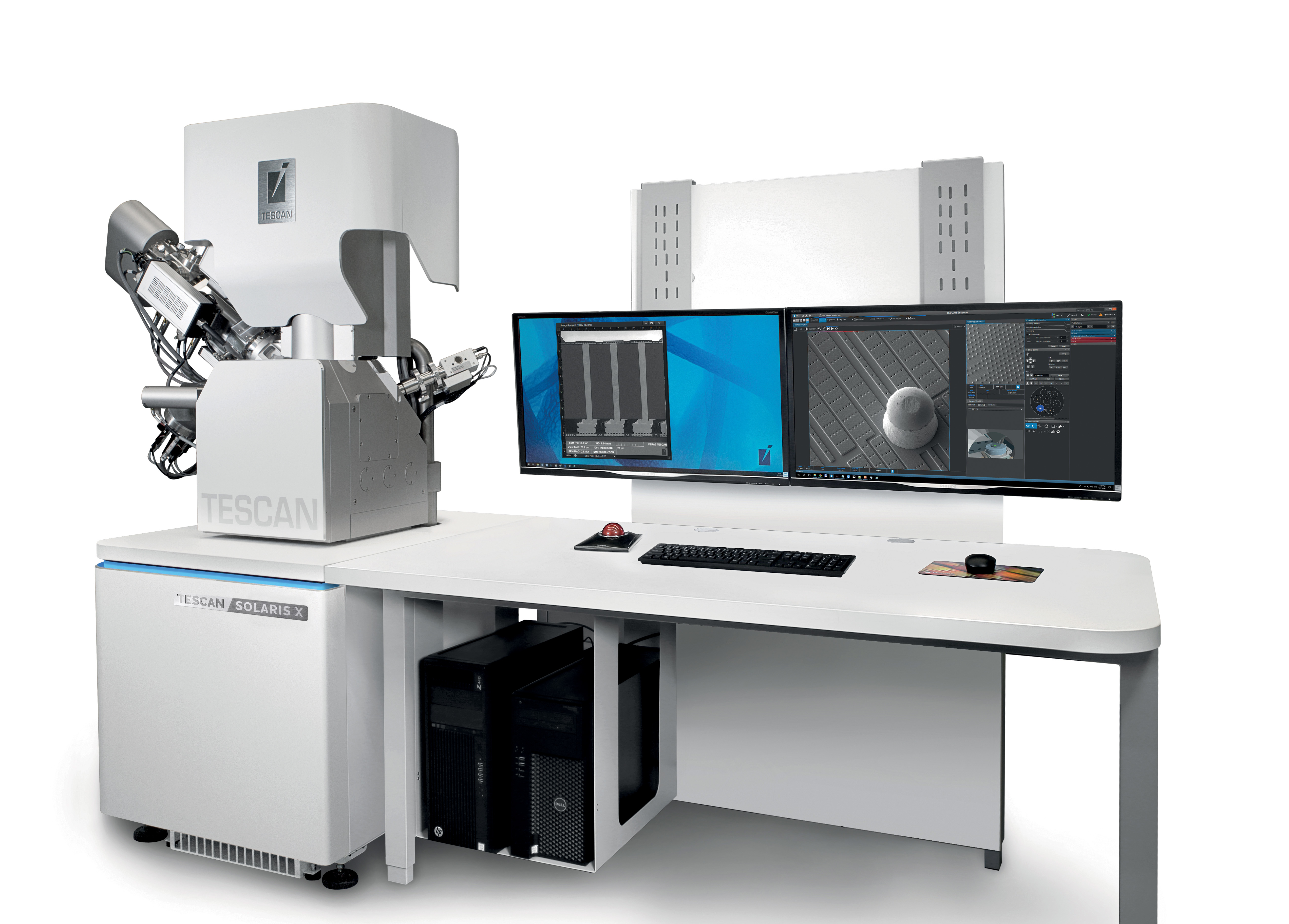
TESCAN ORSAY HOLDING a.s. has announced the release of the new TESCAN Delayering Module that enables automated gas-assisted top-down delayering using TESCAN SOLARIS X and AMBER X Plasma focused ion beam (FIB) instruments. TESCAN Delayering supports physical failure analysis through the combination of inert Xe plasma FIB ions and unique, proprietary gas chemistries that have been developed specifically for today’s advanced technology nodes, creating artifact-free, site-specific trenches—with maximum planarity and homogeneity and without altering a device’s electrical properties—for rapid access to deeply buried features or defects.
“Efficiently delayering today’s devices requires solutions that are different from the standard gas chemistries or traditional gallium (Ga) FIB technologies that have been used in the past for this application,” states Lukáš Hladík, product manager for FIB-SEM in TESCAN‘s Semiconductor market segment. “With TESCAN Delayering, we have developed a state-of-the-art solution for technology nodes below 10nm, and which also provide the ability for users to customize parameters for their own devices. Predictable, automated and unattended delayering can help with allocating and deploying lab resources. Users can be confident that the delayering process will terminate at the designated layer so they don’t need to spend a lot of time monitoring the process.”
TESCAN Delayering uses a step-by-step guided wizard to set-up the required delayering process. Factory-defined templates assure consistent application of all delayering parameters. The templates also can provide the starting point for users to develop their own recipes customized to their specific devices. Once the job is set-up, the TESCAN Delayering module executes the process automatically, with the plasma FIB providing rapid material removal, without Ga implantation or beam damage. At any time during the delayering process, users may monitor the progress by using signal peak recognition in the end-point-detection curve.
TESCAN Delayering module is supported by a team of skilled applications scientists who can assist with process development and customizations for users who want to further streamline their delayering processes.


