

Merck meets demanding customer requirements through revolutionary materials science
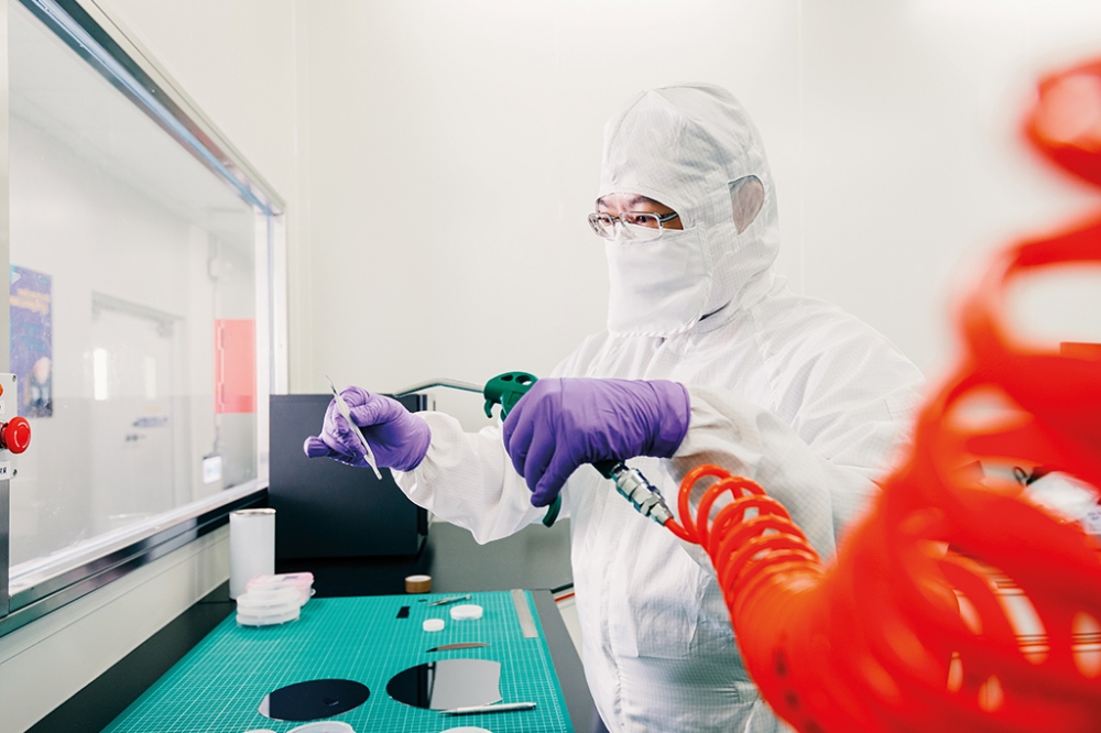
The continuing evolution of semiconductor devices has challenged materials suppliers to take a more active role in defect elimination and yield enhancement as IC manufacturing grows increasingly complex. MERCK, a science and technology company headquartered in Darmstadt, Germany, offers insights into how the company has redefined material science to speed up production, increase yields and provide customers a competitive edge.
DEMANDING PRODUCTION requirements for advanced node semiconductors continue to make the world’s most complex manufacturing processes all the more challenging. Flaws that were inconsequential two or three device generations ago today are ‘killer’ defects in devices at 10nm and below.
As a consequence of ever more stringent process requirements, manufactures and their supporting supply chain members are seeking ways to make the production of advanced node devices as fool-proof as possible. One way to minimize defects requires greater materials purity and precisely controlled formulations that essentially create materials with carefully documented ‘fingerprints’ for each compound so that batches can be more readily sourced, stored, and tracked from the point that they enter the manufacturing process stream to
the very last back end of line steps.

No compound is exempt from constantly improving quality control demands since manufacturers appreciate that the more control they exert over every aspect of a material’s composition, the less likely it is that one of those materials might accidentally inject defect-inducing qualities. At stake is billions of euros in microelectronic devices and trillions in end-use products that will succeed or fail based on their semiconductor content.
The continual advancement of materials science has created unique opportunities for suppliers and process chemical manufacturers that already have stringent standards and exemplary quality controls. Such companies are ideally positioned to meet the growing needs of semiconductor device makers. Somewhat like semiconductor manufacturing, the development and formulation of pharmaceutical and life science products require extreme precision and rigorous quality control. So it should come as no surprise that a company known for quality and advanced technology such as Merck would continually invest in its advanced electronics materials division.
Today, Merck has emerged as one of the largest international players supplying high-purity/high-quality semiconductor process chemical formulations to a growing list of global IC manufacturers.
Merck isn’t satisfied to rest on its laurels or expect its more than 300 years of industrial excellence to meet every requirement in an ever-changing 21st-century global marketplace. Since 2007, Merck has made acquisitions and divestments totaling around Ä40 billion – in the process, Merck has transformed itself into a leading science and technology company supporting semiconductor manufacturers in addition to its prominence in healthcare and life science industries.
Recent acquisitions by Merck include bringing Versum Materials into its family of companies in October 2019. In September that same year, Merck completed its acquisition of Intermolecular, a California-based company focused on advanced materials innovation. Both acquisitions added products, processes, and a wealth of experience to Merck’s already deep well of high performance materials expertise.
Following completion of the Versum acquisition, former Chairman of the Executive Board and former CEO of Merck, Stefan Oschmann remarked, “By acquiring Versum, we will be optimally positioned to capitalize on long-term growth trends in the electronic materials industry. At the same time, we are broadening our commitment to electronic materials, balancing our portfolio with three strong business sectors and sharpening our strategic focus on innovation-driven technologies.”
Echoing those remarks, Kai Beckmann, Executive Board member of Merck and CEO of Electronics said, “We are very pleased to welcome Versum to our team. After the most recent acquisition of Intermolecular, this closing marks another major milestone on our Bright Future transformation journey to become a leading player in the electronic materials market. The expertise of our combined business will enable us to offer customers in the electronics industry cutting-edge technology innovations.”
In all its acquisitions, Merck has sought to add strategic advantages that complement its existing global portfolio. Amongst key benefits of its 2019 acquisition of Intermolecular was an opportunity to relocate the Merck Silicon Valley Innovation Hub team in Menlo Park to Intermolecular’s 150,000 square foot facility located in San Jose, California. Much more than just a consolidation, the move to San Jose allowed Merck to take advantage of Intermolecular’s 30,000 square feet of cleanroom, chemical laboratories, offices, meeting and event spaces in a way that not only benefitted Merck, but also created a unique space to empower collaboration with startup companies focused on advanced materials and support services for semiconductor manufacturing.
“The mission of the Silicon Valley Innovation Hub is to identify and explore untapped innovation and business opportunities for Merck. In this context, the intersection of life science and material science is becoming increasingly important and opens new areas of innovation. Having the Silicon Valley Innovation Hub and Intermolecular under one roof now will allow us and our cooperation partners to develop and test new materials for biological applications. We are very excited about these new opportunities,” stated Thomas Herget, head of the Silicon Valley Innovation Hub, on the occasion of the move by Merck staffers to San Jose in March 2021.
Materials science can and does play a decisive role in the fabrication of next-generation semiconductors. Products and processes that may have previously been considered secondary to the success of a new wafer production step have now proven critical. Equally important is the need for manufacturers to understand and appreciate exactly what constitutes a successful new material or process compared to legacy approaches.
One area in which Merck continues to excel and set new standards involves delivering superior materials as well as better performance data compared to competing approaches. A ready example can be found in the chemical mechanical planarization (CMP) technologies that are utilized throughout the transformation of a bare silicon wafer into a substrate bearing finished devices at high yield with high performance. Amongst its many functionalities in device manufacturing, CMP plays a critical role in producing finished copper interconnects. In production,sheet resistance (Rs) of copper interconnects are measured after the barrier layer is removed by copper/barrier CMP. But generally speaking, this analysis is not available in the laboratories of consumable CMP suppliers.
A combination approach to measuring the effectiveness of CMP on copper interconnects is to examine dishing and erosion following planarization completion. Ordinarily, only dishing is analyzed in part due to the challenges of measuring both qualities.
Merck has found that as feature sizes become even smaller, traditional CMP metrology becomes more time consuming, noisy and challenging. Hence, electrical testing provides the most comprehensive, accurate, and reliable dataset. Merck performs back end of line (BEOL) copper and copper-barrier CMP slurry testing on an electrically capable test vehicle. The test vehicle is then sent to the company’s in-house electrical characterization laboratory.
An automated high-throughput program can be used to probe the test vehicle. For example, 16 features across 32 dies can be measured in four hours, whereas by physical methods (AFM, profilometer), only 11 features across three dies can be measured, which typically takes double the time, (i.e., 8 hours.)
Merck can provide such data to customers upon their request; other CMP suppliers do not have access to such electrical characterization, and typically lack expertise in electrical data analysis. Merck’s approach was developed in concert with customers to ensure that the data made available is not only useful, but provides the manufacturer with an ‘edge’ compared to other approaches to characterizing post-CMP effectiveness.
One company that has partnered with Merck is UMC Fab12i (Singapore.) Fab Director Steven Hsiao shared his opinion that the accelerated success of a recent wafer run could be tied not only to the support of his internal engineering team and production technicians, but also the direct support of Merck in assessing the performance of their CMP copper planarization processes. “We believe that anything is possible if we work together, and we look forward to working with Merck again on our next project,” said Hsiao.
For BEOL copper bulk slurries, Merck products offer the following advantages:
- Tunable profile and dishing to meet customer’s technical requirements, low step-height to large step-height
- Low abrasives to provide low defects
- No pad stains
- High selectivity
- Slurry in corrosion-free regime of the Pourbaix diagram
- Newtonian and Prestonian behavior for predictability across consumable sets
For BEOL copper barrier slurries, Merck products offer the following advantages: - Customized tunable selectivity, working with customer-specific requirements
- Low defectivity
- Superb topography control
- More concentrated formulations
- Compatible with novel liner schemes
“Merck is pushing boundaries to create next-generation CMP slurries which revolutionize the semiconductor industry. The integration of Merck and Intermolecular provides more value to customers and enables us to partner with customers to solve current and future integration challenges. For example, Merck developed its new, innovative CMP slurries and can provide dishing/erosion (physical) data of materials as well as electrical data to measure CMP slurry performance. This preview of electrical data minimizes risk, maximizes yield and shortens cycle time for our customers, which also demonstrates Merck to be a total solutions provider. At Merck, we are striving to respond quickly to industry challenges. We aim to deliver the total solution, and strive to be the preferred partner for our customer’s future needs,” said Laura Matz, the Chief Science and Technology Officer at Merck.

In an effort to continually improve its already industry-leading approach to combining high-performance materials with actionable performance data, Merck is also examining the development of novel abrasives and the ability to modify the surface of abrasive constituents so that materials are effectively customized to a manufacturer’s unique needs and requirements. This is a key element of topography and defect control that will continue to grow in importance as the industry moves from one device generation to the next. Merck has set its sights on leading the semiconductor materials industry; Merck is well down the road to accomplishing its goal.


