5G, AI & IoT devices benefit from the latest dual-layer materials
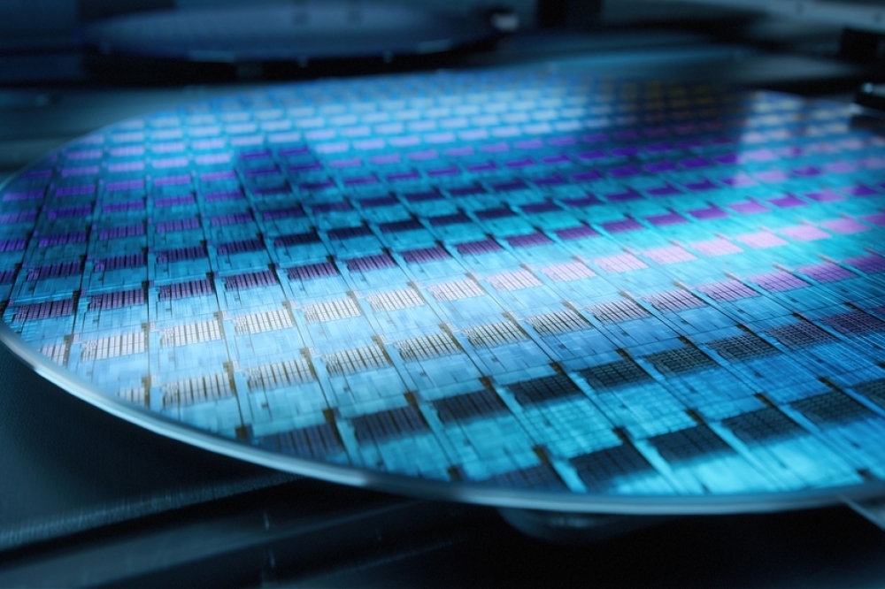
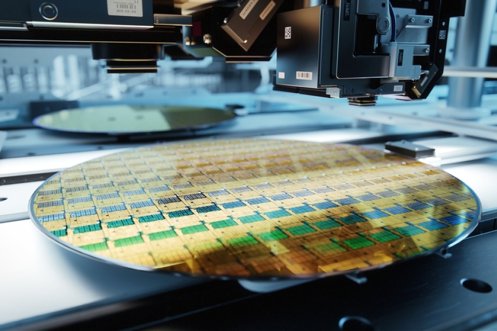
Wafer-level packaging (WLP) has become the norm for a growing number of 5G, Artificial Intelligence (AI) and Internet of Things (IoT) system components. Advanced applications require high-performance integrated circuits (ICs) built on substrates that require extreme thinning. The manufacturing of these devices requires minimal total thickness variation (TTV), little to no warpage, and high temperature survivability during downstream processing. The materials experts at Brewer Science explain how their BrewerBOND Dual-Layer materials and process gives manufacturers the edge they need to lower costs, enhance performance capabilities and increase production throughput.
SUCCESS in creating next-generation electronic devices demands a sound foundation. While the largest IC makers are pushing CMOS scaling to 5 nm and below, other advanced circuit manufacturers are taking different routes to high performance, including the adoption of 2.5D/3D architectures that reduce footprints while increasing processing speed and functionality.
Manufacturers have succeeded in dramatically reducing TTV and warpage while containing costs even as they maintain high throughput. A variety of wafer thinning techniques and material technologies have been developed to enable the support of advanced packaging platforms. One common process is wafer-level chip-scale packaging (WLCSP) that delivers high performance at low cost. But since it utilizes a ‘substrateless’ package, applications can be limited due to die size. As dies continue to shrink, manufacturers are already seeking alternatives. Fan-out wafer-level packaging (FOWLP) technology is seeing continual development since input/output (I/O) density can be increased by fanning out interconnects to external pad locations – this enables a smaller form factor with decreased power consumption.
An important aspect of advanced wafer-level packaging involves the use of temporary wafer bonding (TWB) materials and processes that enable partially processed wafers to withstand various subsequent steps even at very high temperatures and with high vacuum. If asked to describe their ‘ideal’ TWB materials solution that can save time and money while maintaining top performance, many manufacturers would ask for materials that can be applied and bonded at room temperature and can deliver protection when thinned wafers are manipulated as part of thermal compression bonding (TCB) steps. The materials should also be sufficiently flexible to support different cure options while preserving device feature integrity. At the same time, materials should enable the debonding of thinned wafers from carriers using a variety of separation technologies.
“Brewer Science is constantly working to improve its materials that are already seeing widespread adoption. A good example is our Dual-Layer materials that continue to see refinements that make them even more adaptable. We are seeing particular interest from manufacturers developing devices and systems for 5G, AI and IoT applications. Since the intial introduction, Brewer Science Dual-Layer materials have demonstrated protection during thin wafer handling in TCB processing. We continue to improve TTV performance in production environments and we have seen Dual-Layer materials successfully support wafers thinned to 10 µm. They can also be applied at room temperature with any of the industry’s most commonly utilized dispense equipment,” said John Massey, Principal Field Applications Engineer.
Handling thinned wafers is a major challenge within semiconductor manufacturing. Silicon wafers thinner than 50 µm or those with redistribution layers (RDLs) created using a RDL-first process are delicate and expensive to manufacture. Safe handling necessitates the use of support substrates and processing steps that employ temporary bonding and debonding (TBDB) materials designed to enable complex packaging architectures.
Materials created using high-viscosity, low-Tg thermoplastic polymers are commonly used in TBDB processes. When paired with a supportive carrier, these materials offer thermo-mechanical stability and easier handling of thin device substrates. While the extensive selection of TBDB materials offered by Brewer Science supports many bonding/debonding techniques (predominantly: mechanical, laser, and thermal slide), the introduction of higher-temperature steps can cause traditional adhesive materials to behave more like a liquid; as a result, temporarily bonded wafers lose mechanical stability as melt viscosity decreases. This allows some material to soften, weakening bond-line stability. Deformation and delamination of the device wafer can occur at higher temperatures, which leads to downstream processing issues. Brewer Science has developed advanced materials and processes, providing customers a TBDB system that eliminates common material failure points.

Figure 1: The Brewer Science TBDB process flow using Dual-Layer materials.
BrewerBOND® Dual-Layer materials for TBDB
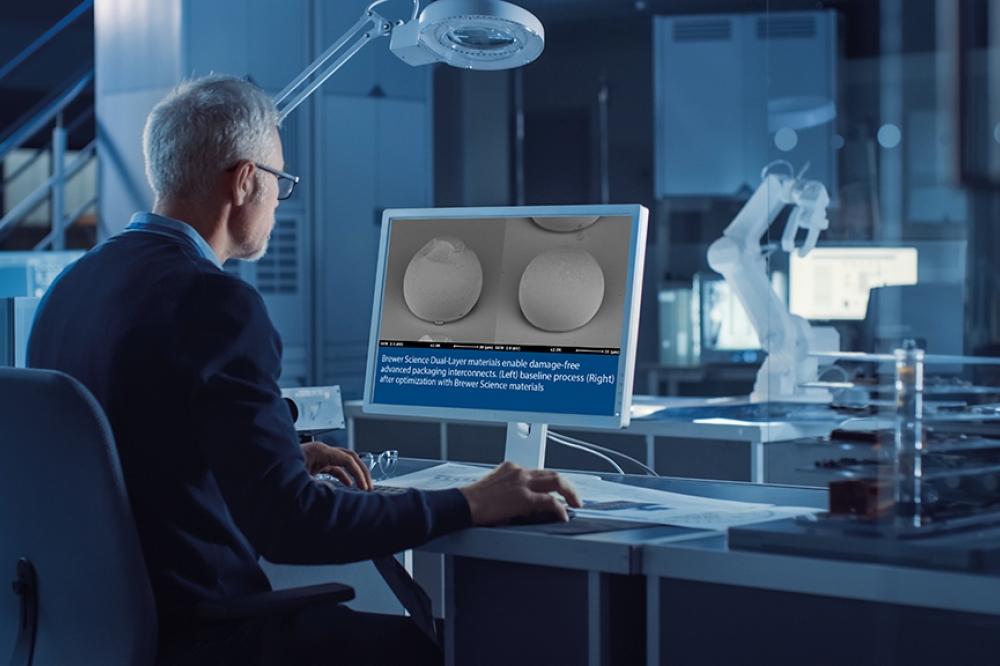
The latest Brewer Science Dual-Layer materials deliver next-generation bonding system performance for high throughput and thermal stability. The materials also provide room-temperature bonding and debonding for both wafer-level and panel-level processing. Dual-Layer materials support wide-ranging manufacturing requirements, enabling more uniform post-grind device thicknesses of < 50 μm while also enabling device structures (and the temporary bond) to survive high-temperature treatments under vacuum. Figure 2 shows a scanning electron microscope (SEM) image of damage-free device features enabled by Brewer Science Dual-Layer materials and process optimization (left). The same size features using the baseline process are shown on the right.

Figure 2: Scanning electron microscope images showing damage-free device
features enabled by Brewer Science Dual-Layer materials and process
optimization (left) and defects found in the same-sized features (right)
that were made using the baseline process.
According to Kim Yess, Brewer Science Executive Director for Wafer-Level Packaging Materials, the Dual-Layer approach of BrewerBOND materials has key advantages compared to the previous solutions offered to the industry.
“The BrewerBOND T1100 series materials are designed to conformally coat the device structures before bonding; the materials have specific rheology attributes for exceptional conformal coating for protection of device structures. The BrewerBOND C1300 material is a curable thermoset layer used in conjunction with the T1100 series material, which remains malleable until final cure. This will enable the bonded pair to have very low TTV and also survive downstream processes approaching 400°C,” she said.
Yess explained that the Dual-Layer system includes a low-glass-transition-temperature (low-Tg) thermoset material (BrewerBOND C1300) applied to a carrier. This assembly is then bonded to the device wafer that has been processed with the corresponding higher-Tg bonding material (BrewerBOND T1100) that coats device structures. After bonding and processing at room temperature, the pair can then either be UV exposed or hotplate baked to cure the thermoset material. When processed below 350°C, the BrewerBOND T1100 series material remains solvent-soluble with little to no melt flow up to 300°C. When coated, this material is highly conformal and can cover severe topography even when applied thinly. Figure 3 shows a scanning electron microscope (SEM) cross-section of a 2.15 µm film of BrewerBOND T1100 series material processed over 80 µm solder bumps.

Figure 3: The BrewerBOND T1100 material delivers highly conformal coating and adhesion preperties.
Yess explained that the exceptional performance achieved by their Dual-Layer approach was developed by Brewer Science to optimize the coatings’ most essential qualities while making various application steps fit into typical process flows at high throughput levels. (See Table 1 for key materials properties.)

Table 1: Properties of BrewerBOND advanced materials
“The BrewerBOND T1100 and C1300 materials need each other to perform to their optimal potential. The BrewerBOND T1100 material is thinner, relatively speaking, and more conformal, which manufacturers need to address ever-shrinking device geometries. It also enables easier downstream cleaning of the device. Our BrewerBOND C1300 material creates better stability during higher-temperature processes, which reduces warpage and helps ensure post-processing functionality of the devices being packaged,” she said, noting that using the BrewerBOND C1300 material by itself is only one piece of the process and that the thermoplastic is required for the mechanical debond processes.
“Creation of new device structures and their extreme requirements are stretching the limits of the techniques and materials used up to this point. This is why Brewer Science is focusing on developing better materials and processes to enable device manufacturers to achieve the stability and temperature resistance they need for downstream processing, but still retain the ability to remove the coatings as needed simply by using industry-standard cleaning processes and chemicals. By using the right coatings, semiconductor manufacturers can achieve the stability and temperature resistance they need at nano-scale while still retaining the ability to remove coatings as needed,” she explained.
Summary
Brewer Science brings leading-edge materials expertise to advanced packaging that is paving the way for innovation through the use of new temporary bonding/debonding materials that uniquely support FOWLP technology requirements. When combined into a system, Brewer Science Dual-Layer materials impart improved mechanical stability that reduces the hazards of handling thinned bonded wafers that need to undergo high-vacuum or high-temperature processing. The materials’ conformal nature, room-temperature bonding/debonding characteristics and chemical resistance provide added value and improved performance while reducing cost of ownership.
Dual-Layer materials from Brewer Science also facilitate low-energy laser debond processes that deliver improved protection for the device wafer with low carbon residues, and can also facilitate other debonding methods. As packaging techniques continue to evolve and device geometries shrink even further, Dual-Layer materials have evolved as well, enabling processing wafers thinned to 10 µm. They also protect 3D device structures that are capturing an increasingly large share of overall semiconductor production. Brewer Science continues to develop and deliver advances in temporary bonding and debonding materials to facilitate manufacturers’ requirements while formulating new materials to support emerging device packaging technologies now under development.