
Inspection system offers a 'whole new level of safety and efficiency'
Comet Yxlon presents new inspection system for the semiconductor industry.
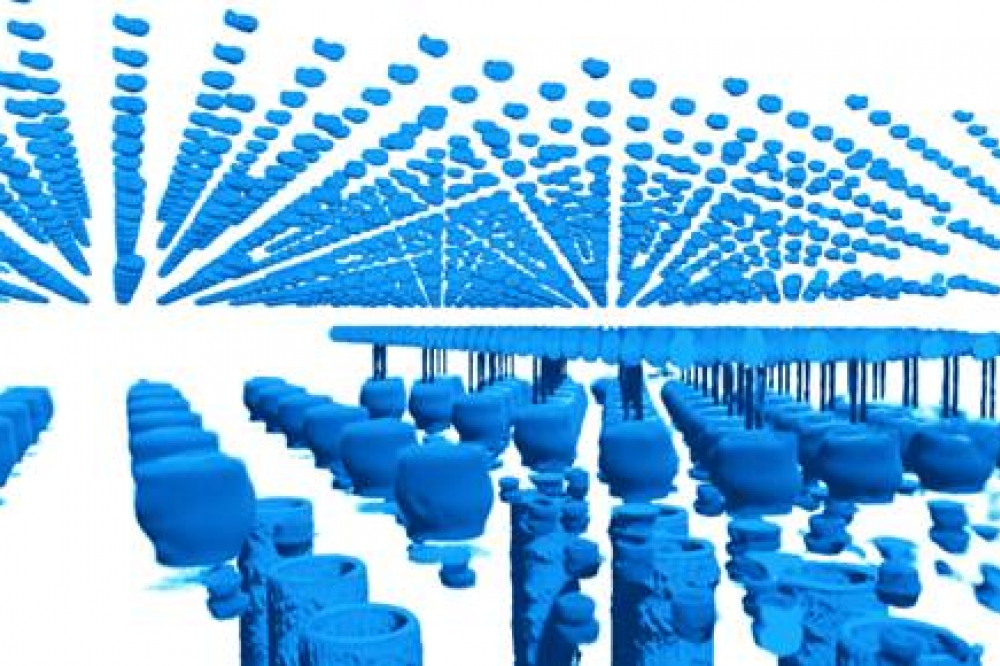
By leveraging advanced computed laminography and integrated AI technology, Comet Yxlon brings high-resolution 3D X-ray capabilities to the forefront for detailed testing in the advanced packaging of integrated circuits. For the first time, the semiconductor market now has a nondestructive supplement or alternative to conventional destructive methods. Three-dimensional X-ray images with a resolution of less than 1 µm can reliably identify typical defects in 3D IC solder connections, such as missing and bridged bumps, voids, non-wet, head-in-pillow, bump shift, and deviations in standoff height or deformations. Modern analysis software based on deep learning takes over the automatic evaluation, including report generation according to the user's requirements. The new CA20 X-ray inspection system, therefore, offers the semiconductor industry a whole new level of safety and efficiency.
Semiconductors have become an integral part of our networked world. That places great demands on manufacturers as innovation cycles are becoming shorter and shorter while the complexity of integrated circuits is constantly increasing. To remain competitive, there is a particular focus on reducing investment costs and accelerating ramp-up processes to achieve error-free production of new, high-performance components more quickly. The early identification of critical defects considerably accelerates the development and optimization of new production processes and thus the production start-up of new chip generations.
With the CA20 inspection system, Comet Yxlon has taken 3D X-ray technology for the semiconductor Advanced Packaging industry to a whole new level. The complete redesign of the hardware, optimized for semiconductor applications in terms of stability, imaging, precision, and maintenance requirements, Comet Yxlon GmbH Page 2 of 3 combined with high-resolution computed laminography and software packages such as Dose Manager, Batch Manager and 'Insights' for automated evaluations ensure accuracy, reliability, and efficiency for all inspection tasks. All functions are easily and intuitively accessed via the Geminy user interface which has proven itself in the Comet Yxlon FF and UX product ranges, equipped with graphical symbols, wizards, and various presets for every skill level.
"As an accompanying inspection method already in research and development of new microchips and their production processes, the new CA20 will revolutionize the semiconductor industry," said Christian Driller, Vice President R&D at Comet Yxlon. "CA20 will ensure that ramp-up processes and time-tomarket are dramatically accelerated, the current high scrap rate will get reduced, and yield will thus significantly increase. The system brings the zero-defect goal within reach."
Yesterday afternoon, Comet Yxlon officially launched the system with live demonstrations and invited guests. During various presentations at the conference, Stephan Haferl (CEO Comet), Dionys van de Ven (President Comet Yxlon), Isabella Drolz (Vice President Product Marketing Comet Yxlon) and Christian Driller had already referred to that momentous event before. The new stand positioning in Hall B2, shared by productronica and Semicon Europa side by side, indicates where Comet Yxlon's journey is heading: The tiniest errors are the biggest challenges in today's world, and Comet Yxlon makes them visible with its technology in line with its promise: 'See better. Faster. More.’


