Semiconductor packaging underfill market to reach $3.4 billion by 2033

The primary growth driver for the Semiconductor Packaging Underfill market is the escalating demand for advanced consumer electronics and the widespread adoption of miniaturized, high-performance semiconductor devices. As electronic devices become increasingly compact and complex, the need for robust underfill materials that enhance the mechanical strength, thermal cycling reliability, and longevity of semiconductor packages has become critical. This trend is further amplified by the proliferation of IoT devices, automotive electronics, and the rapid evolution of 5G technology, all of which require innovative underfill solutions to ensure device reliability and performance.
Introduction: The Invisible Layer That Holds Chips Together
When people talk about semiconductors, the spotlight usually falls on fabrication plants, nanometer nodes, or advanced processors. But beneath every reliable chip—especially those powering EVs, smartphones, telecom networks, and defence systems—lies a quiet hero: semiconductor packaging underfill.
In India’s journey toward becoming a global semiconductor hub, underfill materials are emerging as a critical enabler of performance, reliability, and long-term durability. Though invisible to the end user, underfill technology decides whether a chip survives India’s heat, vibration, and long operating cycles—or fails prematurely.
Understanding Semiconductor Underfill: Beyond Just an Adhesive
What Is Underfill in Semiconductor Packaging?
Underfill is a specialized polymer material injected between the silicon die and the substrate after flip-chip bonding. Its core purpose is to strengthen mechanical integrity and protect solder joints from stress caused by temperature variations and physical shock.
Why Underfill Matters in Indian Operating Conditions
India’s electronics operate in:
• High ambient temperatures
• High humidity zones
• Continuous usage environments (telecom towers, EV power systems, railways)
Underfill compensates for thermal expansion mismatch between silicon and organic substrates—making it indispensable for Indian applications.
Market Drivers: Why the Underfill Market Is Gaining Momentum in India
1. Rise of Advanced Packaging in “Make in India” Electronics
India is shifting from PCB-level assembly to flip-chip, CSP, and wafer-level packaging. These advanced formats cannot function reliably without underfill, making it a non-negotiable material in modern packaging lines.
2. Electric Vehicles and Power Electronics Boom
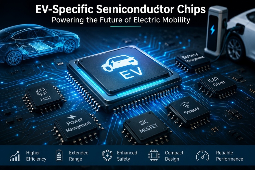
EVs are semiconductor-heavy machines. Power modules, battery management ICs, and inverters demand:
• Thermal stability
• Long lifecycle reliability
• Vibration resistance
Underfill materials directly influence EV safety and longevity, pushing demand upward.
3. Telecom, 5G, and Data Infrastructure Expansion
5G rollout, data centers, and edge computing require high-density packaging with zero tolerance for failure. Underfill ensures signal integrity and mechanical robustness in high-speed chips.
Types of Semiconductor Underfill Materials in Use
Capillary Flow Underfill (CUF)
• Traditional and widely used
• Suitable for high-volume production
• Cost-effective for Indian OSAT facilities
No-Flow Underfill
• Applied before chip placement
• Reduces process steps
• Gaining interest for automation-driven fabs
Wafer-Level Underfill (WLUF)
• Used in miniaturized consumer electronics
• Enables ultra-thin chip packages
• Critical for wearables and compact IoT devices
Material Innovation: Where India’s Opportunity Truly Lies
Epoxy-Based Underfills
Most common due to:
• High adhesion strength
• Thermal resistance
• Cost-effectiveness
Low-Stress & High Thermal Conductivity Formulations
Next-generation underfills are designed to:
• Reduce warpage
• Improve heat dissipation
• Support AI and power-dense chips
This is an open innovation space where Indian chemical and materials companies can play a global role.
India’s Strategic Position in the Global Underfill Value Chain
Government Push & Ecosystem Creation
With semiconductor policies, OSAT incentives, and fabrication roadmaps, India is building end-to-end capability—and underfill materials are a vital link.
Domestic Manufacturing Potential
India already has:
• Strong chemical engineering talent
• Polymer science expertise
• Cost-efficient manufacturing capabilities
Localized underfill production can reduce import dependence and strengthen supply-chain resilience.
Challenges That Demand Smart Solutions
Quality Consistency & Reliability Standards
Underfill performance is measured in microns and microseconds. Indian players must meet:
• Global JEDEC reliability standards
• Automotive-grade qualification norms
Skill Gap in Advanced Packaging Materials
The industry needs:
• Packaging process engineers
• Materials scientists
• Reliability testing specialists
Skill development will determine how fast India scales.
Competitive Landscape
• Henkel AG & Co. KGaA
• H.B. Fuller Company
• NAMICS Corporation
• Hitachi Chemical Co., Ltd.
• Zymet Inc.
• Master Bond Inc.
• Panasonic Corporation
• Shin-Etsu Chemical Co., Ltd.
• Dow Inc.
• Kyocera Corporation
• Dexerials Corporation
• Sunstar Engineering, Inc.
• 3M Company
• Epoxy Technology, Inc.
• Nordson Corporation
• AIM Solder
• Nagase ChemteX Corporation
• Lord Corporation
• Sanyu Rec Co., Ltd.
Future Outlook: Where Is the Market Headed?
Convergence of AI, EV, and Advanced Packaging
As AI accelerators and power electronics converge, underfill will evolve from a support material to a performance differentiator.
Sustainable & Environment-Friendly Underfills
Future formulations will focus on:
• Low-VOC materials
• RoHS and REACH compliance
• Longer lifecycle with lower environmental impact
This aligns well with India’s sustainability goals.
Source:- https://researchintelo.com/report/semiconductor-packaging-underfill-market