
Atomically flat silicon could transform sensors
Silicon is the workhorse of the electronics industry, serving as the base material for the tiny transistors that make it possible for digital clocks to tick and computers to calculate.
Now scientists have succeeded in creating near-atomically flat silicon, of the orientation used by the electronics industry, in a room temperature reaction. The flat silicon might one day serve as the base for new biological and chemical sensors.
"In essence, we have made perfect silicon surfaces in a beaker," says team leader Melissa Hines, a chemist at Cornell University. Researchers had made perfectly flat silicon before, but previous work focused on silicon surfaces cut along a plane of the crystal that is not used in the electronics industry. Hines' team has created the flat surfaces along the industry-standard crystal orientation.
The creation of the team's first near-atomically flat surface came as a bit of a surprise. It was widely believed that the dissolving process the team used to clean the silicon left rough, bumpy surfaces.
Hines was working on a review paper and had asked one of her graduate students to take an picture of the surface using an instrument called a scanning tunnelling microscope (STM) that can image surfaces to atomic-level detail. "When we looked at the surface, we unexpectedly realised, 'Hey, this actually looks very flat,'" Hines says.
The STM is an instrument for imaging surfaces at the atomic level. Its development in 1981 earned its inventors, Gerd Binnig and Heinrich Rohrer (at IBM Zuerich), the Nobel Prize in Physics in 1986. For an STM, good resolution is considered to be 0.1 nm lateral resolution and 0.01 nm depth resolution. With this resolution, individual atoms within materials are routinely imaged and manipulated.
The STM technique is based on the concept of quantum tunnelling. When a conducting tip is brought very near to the surface to be examined, a bias (voltage difference) applied between the two can allow electrons to tunnel through the vacuum between them. The resulting tunnelling current is a function of tip position, applied voltage, and the local density of states of the sample. Information is acquired by monitoring the current as the tip's position scans across the surface, and is usually displayed in image form.
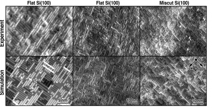
The images above show STM images of flat and miscut NH4F-etched Si (100) surfaces compared to kinetic Monte Carlo simulations of experimental images, rotated to match experimental orientations.
The microscope images initially viewed by the scientists showed a surface with alternating single-atom-wide rows. Using the additional tools of computer simulations and infrared spectroscopy the researchers determined that the silicon atoms in the rows were bonded to hydrogen atoms that acted like a wax, preventing the surface from further reacting once it was set out in the air.
"What that means is that if you take this perfectly flat surface, pull it out of the aqueous reactants, and rinse it off, you can leave it lying around in room air on the order of 10 to 20 minutes without it starting to react," says Hines. "If you had told me as a graduate student that you could have a clean surface that could just hang out in air for 10 minutes, I would have thought you were crazy."
The team believes that part of the reason their silicon surfaces are so flat is that they dip the wafers in and out of solution approximately every 15 seconds, preventing bubbles from the reaction from building up and causing uneven etching. However, they also credit the STM images for helping them to realize just how flat the surfaces were. The team built off the information from the images by using computer simulations and other tools to reveal the exact chemical reaction steps that took place in solution.
"Experimentally, this is very simple experiment: you take a piece of silicon, you swirl it in a beaker with solution, and then you pull it out and look at it. To be honest, there is no reason to think that Bell Labs did not make a surface as good as ours twenty years ago, but they did not look at it with STM, so they did not know," says Hines.
Hines' team is now working on adding molecules to the atomically smooth, hydrogen-terminated silicon surface in the hopes of building new chemical or biological sensors. "At this point, I can't tell you exactly how we will accomplish this, but we have promising results and hope to be able to report more soon," says Hines.
The researchers will present their work at the AVS 59th International Symposium and Exhibition, held between October 28th and November 2nd in Tampa, Florida.


