
Jordan Valley X-ray tool ramps up 14nm & 10nm semiconductor market
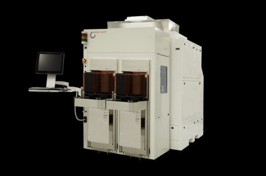
Jordan Valley Semiconductors has received another order for its recently introduced JVX7300LMI scanning X-ray in-line metrology tool for patterned and blanket wafers.
The system has been purchased for advanced process development and production ramp-up for 14nm and 10nm nodes.
The tool provides fully automated advanced metrology for epitaxial materials such as SiGe, Si:C/P and III-V on silicon FinFET structures, as well as high-k and metal gate stacks and other critical layers.
Isaac Mazor, JV CEO, says, "We are pleased to have been selected by key customers to support their FEOL (Front-End-Of-Line) process metrology. This selection represents the customers' confidence in Jordan Valley's ability to provide valuable metrology solutions for their most demanding advanced applications, trusting first principle X-ray based metrology to provide unique process control solutions."
Mazor continues, "Advanced logic devices set new metrology challenges and requirements for key transistor level structure such as FinFET, germanium & III/V materials on silicon, as well as high-k and metal gate stacks used to enhance the transistor performance. Jordan Valley was able to meet the customers' stringent process requirements in a short period of development time.
"In choosing the JVX7300LMI platform, the customers acknowledged the significant contribution of the product in shortening the process development cycle, coupled with enabling process performance and extendibility to future technology nodes." Mazor concludes, "We believe that the JVX7300LMI can be a strong contributor to assure high yield in the current and next generation process nodes."
The JVX7300LMI is a production worthy X-ray metrology system for 14nm & 10nm nodes R&D and production ramp for FEOL applications such as SiGe, Si:C/P, FinFETs, high-k/metal gate and replacement channel materials such as germanium and III-V layers on silicon. It is also used for the development and production of the emerging GaN-on-silicon market.
This tool enables scanning HRXRD, XRR and (GI)XRD measurements. HRXRD is capable of measuring epitaxial layer composition, thickness, density, strain and relaxation of single and multi-layer stacks.
What' more, with XRR and (GI) XRD channels, the tool provides information on the thickness, density, phase and crystallinity of ultra-thin layers typically used in the FEOL process. Unlike optical or spectroscopic tools, the HRXRD and XRR are first principle techniques that deliver accurate and precise results without calibration.


