+44 (0)24 7671 8970
More publications     •     Advertise with us     •     Contact us
 
News Article

SÜSS MicroTec launches mask aligner for packaging

News

The MA12 mask aligner addresses the Advanced Packaging market including 3D wafer-level chip scale packaging and wafer-level packaging and the MEMS market

SÜSS MicroTec, a global supplier of equipment and process solutions for the semiconductor industry and related markets, has launched the Mask Aligner MA12.

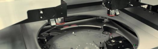
This semi-automated tool is designed for industrial research and production of wafers up to 300 mm and 300 x 300 mm square substrates.

It is one of the latest mask aligner technologies in terms of accuracy, optical performance and versatility.

The operator assisted MA12 offers high process flexibility including submicron alignment and features the MO Exposure Optics of SÜSS MicroTec, a unique illumination optics, adjustable to meet various exposure requirements.

The newly-introduced mask aligner addresses the Advanced Packaging market including 3D wafer-level chip scale packaging (3D WLCSP) and wafer-level packaging (WLP) as well as the MEMS market.

The SÜSS MicroTec MA 12 combines the advantages of a reliable manual tool specialized on the handling of delicate substrates, such as highly warped wafers and fragile substrates, with the performance of a 300mm lithography tool. Processes developed on the MA12 can be quickly transferred onto the automated SÜSS MicroTec MA300 high volume production platform.

"The MA12 has been designed to enable quick and effective development of new products and process technologies", explains Frank P. Averdung, president and CEO of SÜSS MicroTec. "Research organizations will benefit from the enhanced capabilities of the industry-compatible MA12 as it offers the flexibility needed in the development and adoption of latest llithography processes."


Purdue, imec, Indiana announce partnership
Resilinc partners with SEMI on supply chain resilience
NIO and NXP collaborate on 4D imaging radar deployment
Panasonic Industry digitally transforms with Blue Yonder
Global semiconductor sales decrease 8.7%
MIT engineers “grow” atomically thin transistors on top of computer chips
Keysight joins TSMC Open Innovation Platform 3DFabric Alliance
Leti Innovation Days to explore microelectronics’ transformational role
Quantum expansion
indie launches 'breakthrough' 120 GHz radar transceiver
Wafer fab equipment - facing uncertain times?
Renesas expands focus on India
Neuralink selects Takano Wafer Particle Measurement System
Micron reveals committee members
Avoiding unscheduled downtime in with Preventive Vacuum Service
NFC chip market size to surpass US$ 7.6 billion
Fujifilm breaks ground on new €30 million European expansion
Fraunhofer IIS/EAS selects Achronix embedded FPGAs
Siemens announces certifications for TSMC’s latest processes
EU Chips Act triggers further €7.4bn investment
ASE recognised for excellence by Texas Instruments
Atomera signs license agreement with STMicroelectronics
Gartner forecasts worldwide semiconductor revenue to decline 11% in 2023
CHIPS for America outlines vision for the National Semiconductor Technology Center
TSMC showcases new technology developments
Alphawave Semi showcases 3nm connectivity solutions
Greene Tweed to open new facility in Korea
Infineon enables next-generation automotive E/E architectures
Global AFM market to reach $861.5 million
Cepton expands proprietary chipset
Semtech adds two industry veterans to board of directors
Specialty gas expansion
×
Search the news archive

To close this popup you can press escape or click the close icon.
Logo
×
Logo
×
Register - Step 1

You may choose to subscribe to the Silicon Semiconductor Magazine, the Silicon Semiconductor Newsletter, or both. You may also request additional information if required, before submitting your application.


Please subscribe me to:


You chose the industry type of "Other"

Please enter the industry that you work in: