
SEMICON West: KLA-Tencor Reveals Inspection and Review Portfolio
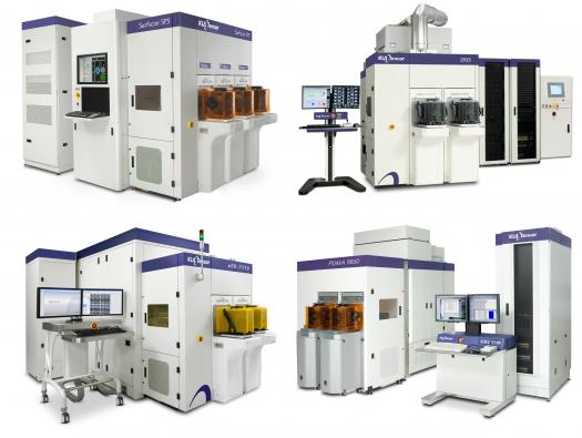
KLA-Tencor Corporation has announced four new systems"”the 2920 Series, Puma 9850, Surfscan SP5 and eDR-7110"”that provide advanced defect inspection and review capability for the development and production of 16nm and below IC devices. The 2920 Series broadband plasma patterned wafer, Puma 9850 laser scanning patterned wafer, and Surfscan SP5 unpatterned wafer defect inspection systems deliver enhanced sensitivity and significant throughput gains. By enabling discovery and monitoring of yield-critical defects, these inspectors support chipmakers' integration of complex structures, novel materials and new processes at leading-edge design nodes. Each of the inspection systems seamlessly connects with the eDR-7110 electron-beam review system, which utilizes improved automatic defect classification capability to quickly identify detected defects, providing chipmakers with accurate information for determining corrective action.
"As our customers integrate many unique technologies at the 16nm, 14nm and smaller design nodes, they face complex yield and reliability challenges," said Bobby Bell, executive vice president of KLA-Tencor's Wafer Inspection Group. "The four systems announced today"”flagship products in our inspection and review portfolio"”incorporate numerous innovations to help solve defectivity issues across a broad range of applications. Our optical inspectors and e-beam review system find and identify critical nanoscale defects, while achieving high productivity for evaluating how these defects vary across a wafer, wafer-to-wafer and lot-to-lot. We believe this portfolio, by producing comprehensive defect information, can help our customers characterize and optimize their advanced processes to accelerate time-to-market."
Utilizing a third-generation broadband plasma illumination source, the 2920 Series patterned wafer defect inspection platform delivers twice the light of its predecessor, enabling the use of a new deep ultra violet (DUV) wavelength band and the industry's smallest optical inspection pixel. Along with new advanced algorithms, these optical modes boost sensitivity to subtle protrusions, tiny bridges and other pattern defects on complex IC device architectures, such as FinFETs. In addition, the 2920 Series' novel Accu-ray and Flex Aperture technologies can quickly determine the best optical settings for capture of critical defect types, significantly reducing the time required to discover and solve process and design issues.
With multiple platform enhancements, the Puma 9850 laser scanning patterned wafer defect inspection system provides improved sensitivity across a range of production throughputs to support a diverse array of FinFET and advanced memory inspection applications. Complementing the 2920 Series inspectors, the Puma 9850's higher sensitivity operating modes facilitate yield-relevant defect capture on after-develop inspection (ADI), photo-cell monitor (PCM), and front-end-of-line line-space etch layers. Higher speed modes, operating at up to twice the throughput of the Puma 9650, allow for cost-effective excursion monitoring in the film and chemical-mechanical planarization (CMP) process modules.
The Surfscan SP5 unpatterned wafer inspector incorporates enhanced DUV optical technologies that produce sub-20nm defect sensitivity at production throughput, enabling detection of tiny substrate or blanket film defects that can inhibit successful integration of multi-stack IC devices. With throughput up to three times faster than the previous-generation Surfscan SP3, the Surfscan SP5 maintains high productivity while qualifying and monitoring the increased number of process steps associated with multi-patterning and other leading-edge fabrication techniques.
The eDR-7110 e-beam review system includes a new SEM Automatic Defect Classification (S-ADC) engine that can produce an accurate representation of the defect population during production and can be used during development to dramatically reduce the time required for defect discovery. Moreover, S-ADC results can automatically trigger additional in-line tests, such as compositional analysis or imaging with alternative modes, while the wafer is still on the eDR-7110"”a unique capability that enhances the quality of the defect information provided to engineers for process decisions.
Multiple 2920 Series, Puma 9850, Surfscan SP5 and eDR-7110 systems have been installed at foundry, logic, and memory manufacturers worldwide where they are being used for development and production ramp at advanced technology nodes.
All four systems are backed by KLA-Tencor's global comprehensive service network.


