
Researchers design liquid crystal to overcome challenges posed by organic field effect transistor materials
Researchers at Tokyo Institute of Technology have designed a smectic liquid crystal that overcomes many of the challenges posed by organic field effect transistor materials.
Crystalline organic semiconductors have attracted a lot of interest for convenient low-cost fabrication by printed electronics. However progress has been stymied by the low thermal durability and reproducibility of these materials. Now researchers at Tokyo Institute of Technology and the Japan Science and Technology Agency have designed a liquid crystal molecule that produces high-performance organic field effect transistors (FETs) with good temperature resilience and relatively low device variability in addition to high mobility.
Hiroaki Iino, Takayuki Usui and Jun-ichi Hanna designed a molecule that would incorporate a number of desirable liquid crystal qualities, in particular the smectic E phase. Low ordered liquid crystal phases form droplets at their melting temperature, but the smectic E phase has the advantage of retaining the thin-film shape.
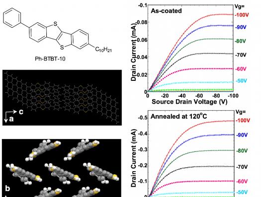
They then fabricated organic FETs by spin coating a solution of their material at 110 °C before allowing it to cool. Comparison of the FET characteristics before and after mild annealing revealed a phase transition. Using atomic force microscopy the researchers identified that at around 120°C in the crystal formed a bilayer crystal phase.
The mobility of a bottom gated FET made from the material was around 12 cm2V-1s-1 comparable to single-crystal devices. "Considering that it could potentially be necessary to fabricate millions of FETs for display applications, polycrystalline OFETs may have an advantage over single-crystal OFETs," point out the researchers in a report of the work. The devices also exhibited a minimal variability of just 1.2 cm2V-1s-1, which is likely an advantage from the smoothness of the obtained film.
The researchers conclude, "The discovery of a dramatic enhancement of FET mobility up to 13.9cm2V-1s-1, resulting from the phase transition from a monolayer to a bilayer crystal structure in mono-alkylated liquid crystalline molecules may lead to the possibility of designing new materials for the burgeoning field of printed electronics."
Background
Small-molecule versus polymer FETs
The main issues around organic semiconductor FETs with small molecules are the low thermal durability. The same bonding that makes the molecules soluble for printing fabrication processes also leaves them prone to low melting points, which greatly inhibits the methods available for processing the materials. They also tend to form rough surfaces, which makes it difficult to reproducibly fabricate the devices that have the desired characteristics.
Attempts to use polymers with benzene-like delocalised electron bonding alleviated issues around the thermal durability to a certain extent. However, it exacerbated others, such as reproducible synthesis and purification of the polymers, as well as control of crystallinity and the molecular orientations towards both the substrate surface and the electrodes.
The design of the molecule
The researchers identified specific characteristics to enrol in the design of their molecule. They used a fused ring system of molecules with benzene-like delocalised electron bonding so that the material would readily crystallise. They then added a phenyl group to introduce the kind of disorder required for smectic E phase liquid crystals. A long flexible carbon chain was also added to encourage formation of a liquid crystal.
The molecule was also designed to have a single side chain so that crystallisation on cooling would be lower than that on heating. This is more convenient for fabrication processes with the material.
The phase transition
Studies of the field effect transistors before and after mild annealing revealed an improvement in carrier mobility by over an order of magnitude. The researchers concluded that the material underwent a phase transition between 70 °C and 120 °C. Improvements in device performance plateaued above 120 °C.
Atomic force microscope studies of the materials identified a step structure that changed from monolayer 2.8 nm steps to bilayer 5.7 nm steps following the phase transition. In the absence of a change in grain size or contact resistance, the researchers concluded that crystal-to-crystal phase change from a monolayer to a bilayer structure was responsible for the improved transistor performance in annealed devices.

Figure caption:
Left: the material chemical structure (top), and single-crystal structures of the ac (middle) and ab planes (bottom). Right: Output characteristics of FETs fabricated using the polycrystalline thin films as-coated (top) and after thermal annealing at 120 °C for 5 min (bottom).


