
Nano-earthquakes' hold key to smarter electronics
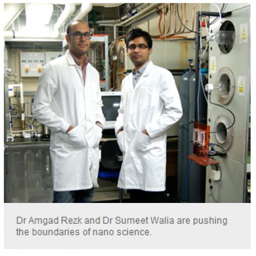
RMIT University's Dr Sumeet Walia and Dr Amgad Rezk have examined the use of sound waves to controllably change the electronic properties of 2D materials, in a study led by Dr Sharath Sriram.
Their work has been published in the summer in the journal Advanced Optical Materials.
The finding has important implications for electronics and optoelectronic devices made from 2D materials, opening the door to a new era of highly efficient solar cells and smart windows.
Other possible fields of applications could include consumer imaging sensors suitable for low-light photography, for example in mobile phone cameras, which currently suffer from poor low-light performance, or in sensors for fluorescence imaging.
Walia, from RMIT's Functional Materials and Microsystems (FMM) Research Group, said atomically thin semiconductors, popularly called two-dimensional (2D) materials, had been known for decades, but their properties were a relatively new and exciting area for nanotechnology, with many promising applications in nanoelectronics and optoelectronics.
Optoelectronic devices are electronic devices that can interact with, as well as control, light. This property can be harnessed for producing ultrasensitive detectors of light and high-speed phototransistors.
The RMIT research looked at ways of using surface acoustic waves or "nano-earthquakes" to control the properties of 2D materials.
"Sound waves can be likened to ripples created on the surface of water, but where we can control the direction and intensity of these ripples," Walia, from the School of Electrical and Computer Engineering said.
"In this work, we use these ripples which occur on a crystal surface and couple it into a material that is a few atomic layers thick (2D material), which causes a change in its electronic properties.
"As the surface acoustic waves are turned on and off or increased and decreased in intensity, the change in electronic properties of the 2D materials follows the same pattern."
Rezk, a member of RMIT's Micro/Nano Physics Research Laboratory (MNRL) and a Research Fellow in the School of Civil, Environmental and Chemical Engineering, said: "A simple technique to control these properties without affecting their inherent chemical and physical characteristics has been a primary scientific hurdle that has hindered their transformation into commercial products.
"We've found that "˜nano-earthquake'-like waves under the surface of the 2D materials drag electrons along their path, thereby tuning the amount of light emitted by the material.
"Remarkably, the acoustic wave based tunability did not result in any structural or compositional change in the material.
"As soon as the acoustic waves were removed, the material retracted back to its initial optical state, and therefore this mechanism is highly adaptable for a variety of dynamically operating systems."
The work is a collaborative effort between MNRL, led by Professor Leslie Yeo, and the FMM Research Group led by Dr Madhu Bhaskaran and Dr Sharath Sriram .
This work was supported by the Australian Research Council and undertaken at RMIT's state-of-the-art MicroNano Research Facility.


