
3D "Nanobridges" Formed Using Electron Beam Writing with Tiny Jets of Liquid Precursor
Researchers have demonstrated a new process for rapidly fabricating complex three-dimensional nanostructures from a variety of materials, including metals. The new technique uses nanoelectrospray to provide a continuous supply of liquid precursor, which can include metal ions that are converted to high-purity metal by a focused electron beam.
The new process generates structures that would be impossible to make using gas-phase focused electron beam-induced deposition (FEBID) techniques, and allows fabrication at rates up to five orders of magnitude faster than the gas-phase technique. And because it uses standard liquid solvents, the new process could take advantage of a broad range of precursor materials. Multiple materials can also be deposited simultaneously.
"By allowing us to grow structures much faster with a broad range of precursors, this technique really opens up a whole new direction for making a hierarchy of complex three-dimensional structures with nanoscale resolution at the rate that is demanded for manufacturing scalability," said Andrei Fedorov, a professor in the George Woodruff School of Mechanical Engineering at the Georgia Institute of Technology. "This could provide a fundamental shift in the way this field will go."
The research was supported by the U.S. Department of Energy's Office of Science and reported in the journal Nano Letters. Applications for the rapid electron beam writing of topologically complex 3D nanostructures could include new types of electrode topologies for batteries and fuel cells, vertically-stacked electronic memory, substrates for controlling cell differentiation and tiny electrochemical conversion devices.
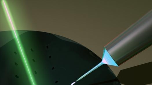
In the established FEBID process, an electron beam is used to write structures from molecules adsorbed onto a solid surface that provides support and nucleation sites for deposit growth. The precursors are introduced into the high-vacuum electron microscope chamber in gas phase. High-energy electrons in the beam interact with the substrate to produce the low-energy secondary electrons, which dissociate the adsorbed precursor molecules, resulting in deposition of solid material onto the substrate surface.
Though it enables precise atom-by-atom fabrication of nanostructures, the process is very slow because the low density of adsorbed gas molecules in the vacuum environment limits the amount of material available for fabrication. And structures must be fabricated from the substrate surface up at continually decreasing growth rate and from a limited number of precursor gases available.
Fedorov and his collaborators have dramatically accelerated the process by introducing electrically-charged liquid-phase precursors directly into high vacuum of the electron microscope chamber. Liquid-phase precursors had been demonstrated before, but the materials had to be enclosed in a tiny capsule where the reaction took place, limiting fabrication flexibility, capacity and utility of the approach for 3D nanofabrication.
The research team "“ including graduate student and first author Jeffrey Fisher, postdoctoral fellow Songkil Kim and senior research engineer Peter Kottke "“ used low volatility solvents such as ethylene glycol, dissolving a salt of silver in the liquid. In solution, the salt dissociates into silver cations, allowing production of silver metal deposits by electrochemical reduction reaction using solvated secondary electrons rather direct molecular decomposition.


