
EV GROUP rolls out automated metrology system for advanced packaging, mems and photonics manufacturing
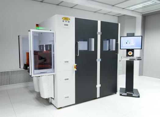
EV Group (EVG), a supplier of wafer bonding and lithography equipment for the MEMS, nanotechnology and semiconductor markets, has introduced the EVG50 automated metrology system. Designed to support the increasingly stringent manufacturing requirements for advanced packaging, MEMS and photonics applications, the EVG50 performs high-resolution non-destructive multi-layer thickness and topography measurement, as well as void detection, in bonded wafer stacks and in photoresists used in optical lithography. The system measures layers down to two microns in thickness, can inspect up to one million points, and achieves throughputs of up to 55 300-mm wafers per hour. This combination of extremely high resolution and high throughput provides cost-efficient full-wafer inspection that enables device manufacturers to improve their wafer bonding and lithography processes, as well as achieve higher yields.
Dr. Thomas Glinsner, corporate technology director at EV Group, noted, "The semiconductor industry is witnessing a trend toward total control and monitoring of all production processes. Mid-end-of-line and back-end packaging processes face tighter process constraints at levels previously seen only in front-end-of-line wafer processing. This is creating an urgent need for highly accurate in-line metrology that can provide critical process data quickly and cost-effectively. The EVG50 is an important addition to our suite of metrology solutions that achieves these goals at speeds and resolutions that far surpass those of competitive systems."
The standalone EVG50 system was developed based on the company's existing in-line metrology module (IMM), which is available as an option in EVG's line of 300-mm process equipment and has been widely implemented in high-volume manufacturing. The EVG50 complements the company's versatile EVG40NT measurement system, which is the industry standard for bond overlay inspection, to meet increased customer demand for full-area layer thickness and topography measurement in critical applications. The EVG50's high throughput and unparalleled accuracy and repeatability, even at ultra-high resolutions, enables cost-effective, 100-percent inspection of production wafers, resulting in improved process control.
The EVG50's versatility allows it to measure coating thickness for lithography as well as wafer bow and warpage, and make void inspections for a bonded wafer stack on the same system, while its low-contact edge handling enables particle-free, full-area wafer inspection. Another key benefit of the EVG50 is its flexibility. Leveraging a multi-sensor measurement mount, the system can be customized for different thickness ranges and substrates to address a wide variety of customer requirements. Its self-calibration capability also allows for better system reproducibility and productive uptime.


