|
View this message online
|

|
|
Newsletter:
24th June 2025


|
|
|
|
|
|
|
|
|
|
|

|

Advanced fabs require more innovative facility services for efficiency, reliability and resiliency
Today’s fabs are highly complex environments that demand
precision, reliability, and real-time adaptability. Industry success will
depend on a stable workforce with specialised skills, a keen eye on processes
and efficiencies, and a commitment to embracing innovative facility management
partners and solutions.
By Joseph Cestari, Vice President, Semiconductor Operations
and Neha Dhingra, Vice President, Semiconductor Strategy at ABM
|
|
|
|
|
|
|
VIDEO INTERVIEW
|
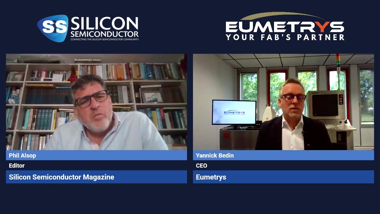
Eumetrys measures up to industry challenges
Yannick Bedin, CEO of Eumetrys, discusses the company’s metrology expertise, looking at the ways in which it is helping its customers to address the key challenges and opportunities they face within the semiconductor industry – with advanced packaging, compound semiconductors and the need for faster and more...
|
|
|
|
LATEST ON-DEMAND WEBINAR
|

Delivering a Maintenance-Free Feedback Solution with Battery-less Energy Harvesting Encoder
Presenting energy harvesting technology and highlighting Broadcom´s AS20-M42M series absolute encoder: Battery-less multi-turn counter integrated to a magnetic single-turn ASIC. The innovative solution is packed into a miniature 20mm diameter with built-in protocol options: SPI/SSI/BiSS-C/RS485.
|
|
|
VIDEO
|
|
|
Eumetrys measures up to industry challenges
Yannick Bedin, CEO of Eumetrys, discusses the company’s metrology expertise, looking at the ways in which it is helping its customers to address the key challenges and opportunities they face within the semiconductor industry – with advanced packaging, compound semiconductors and the need for faster and more...
|
|
NEWSLETTER SPONSOR: ULVAC

Advanced Plasma Resist Strip System
The ENVIRO-1Xa photoresist removal equipment from ULVAC, offers superior performance at an exceptional price. The system can handle multiple wafer sizes, ranging from 100 to 200 mm in diameter. The system utilizes a high efficiency downstream plasma source and can achieve ash rates >10µm/min, with a throughput of 70+wph. This is all achieved on a minimal footprint of 1.57m2. It offers high process flexibility that is required for demanding processes, such as: high-dose implanted resist removal, descum and surface modification, SU-8 and fluorinated resist removal, and MEMS sacrificial-layer removal.
|
 |
| Silicon Semiconductor China |
Volume 2025 - Issue 4/5
Providing in-depth analysis and timely reports on the global industry for its 10,000 professional readers in China
|
|
|
Silicon Semiconductor MAGAZINE
CORPORATE PARTNERS
Why not join our Corporate Partners?
Your logo will appear on every page of the Silicon Semiconductor Magazine website, every edition of the
weekly email newsletter and all 5 editions of our magazine. Join today and receive fantastic visibility
to the Silicon Semiconductor Industry.
|
|
|
|
|
Silicon Semiconductor magazine delivers keen insight into new and evolving technologies, and how they shape tomorrow's futures, and fortunes.
|
|
We hope that you found this newsletter of interest. If not, you may easily
unsubscribe or manage your preferences here.
[COMPANY_ADDRESS]
|