Why the global semiconductor industry needs SEMI EDA standards

By improving data throughput and seamlessly integrating with modern analytics and artificial intelligence-driven solutions, standards enable real-time process optimisation, predictive maintenance, and more adaptive manufacturing operations.
BY DR. FAHAD GOLRA, DIRECTOR OF PRODUCT INNOVATION, AGILEO AUTOMATION
Since the development of SEMI Equipment Communications Standard 1 (SECS-I) in the early 1980s, SEMI has continually advanced the standardization of semiconductor manufacturing. SECS-I laid the groundwork for communication between semiconductor manufacturing equipment and factory systems.
Over the years, SEMI has expanded its portfolio with SECS-II, GEM (Generic Equipment Model), and the GEM300 standards suite. These standards provide a common language for communication, data exchange, and control between shop-floor equipment and IT systems. By standardizing these interactions, SEMI has enabled seamless integration of equipment from multiple vendors, an essential requirement in wafer fabrication facilities. SEMI standards now underpin key activities such as equipment communication, process control, material management, and data collection
The evolution from SECS/GEM to EDA
More recently, SEMI introduced Equipment Data Acquisition (EDA), often referred to as Interface A, to expand its standards suite and address the semiconductor industry’s increasingly diverse and complex needs. EDA standards facilitate and streamline communication between a factory’s data collection applications and manufacturing equipment.

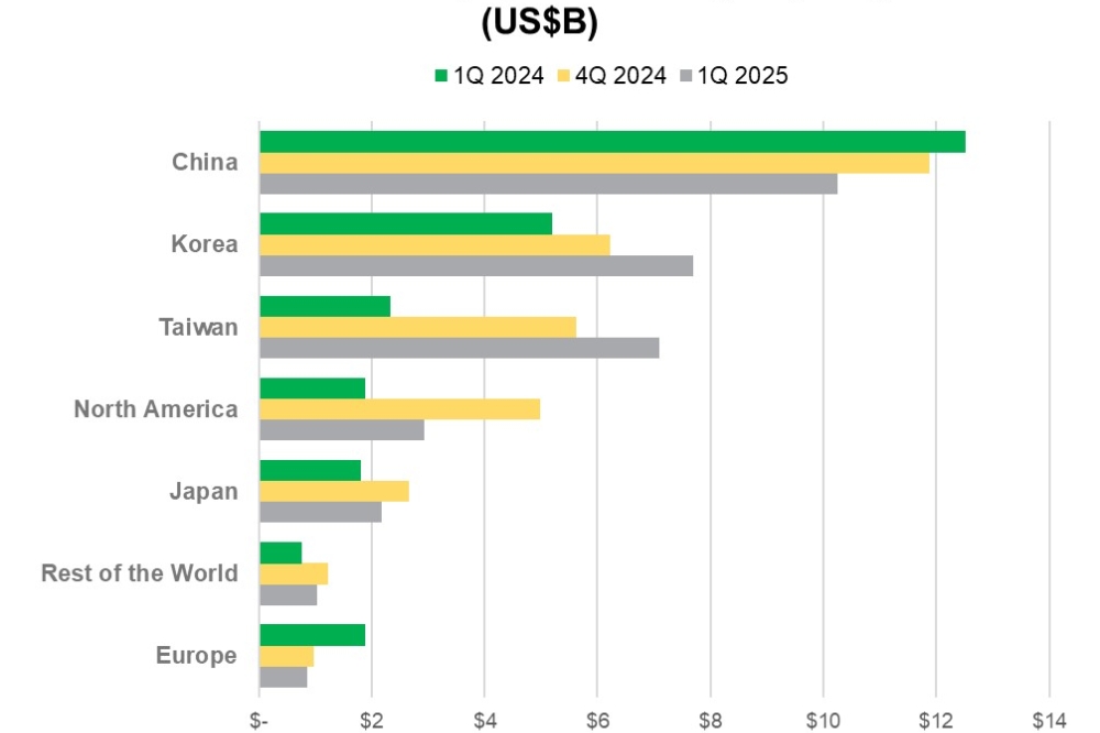
EDA Freeze 2 & 3 standards suite mappedto GEM/ GEM300 standards
The evolution from SECS/GEM to GEM300 and now EDA is a natural progression that reflects the increasing complexity of semiconductor manufacturing. The original SECS/GEM standards established a robust framework for equipment-to- host communication and standardized equipment behavior, enabling reliable interactions and laying the foundation for automation. With the move from 200mm to 300mm wafers, GEM300 was introduced to address higher throughput requirements and advanced process control. Building on SECS/GEM, GEM300 added features such as job management, automated material handling, and material tracking that were critical to support larger wafers and increased production volumes.
As industry scaled up, the importance of data collection and utilization became paramount. The EDA (Interface A) suite emerged as a solution for high-speed, high-volume data acquisition.
Complementing SECS/GEM and GEM300, EDA enables real-time data analysis, process optimization, and predictive maintenance which are vital for data-driven manufacturing.
Together, SECS/GEM, GEM300, and EDA provide a comprehensive roadmap for improving efficiency, yield, and quality control. This evolution ensures that semiconductor fabs remain competitive, highly automated, and ready to innovate in an ever- evolving market.
Leveraging equipment data for fab efficiency
Modern semiconductor equipment generates large volumes of real-time data that underpin a wide range of critical applications, including:
Run-to-run control (R2R): Dynamically adjusts equipment settings to maintain consistent output quality between production runs.
Fault detection and classification (FDC): Monitors data to detect and classify anomalies, preventing defects.
Virtual metrology: Predicts process parameters using sensor data, reducing the need for physical measurements and improving throughput.
Condition monitoring: Analyses equipment and sensor data to predict and prevent failures, minimizing unexpected downtime.
Data analysis: Identifies patterns and trends to optimize processes, improve yields, and increase overall efficiency.
These data-driven applications illustrate the transformative impact of harnessing equipment data. By implementing robust data collection standards, fabs can operate with greater agility, solve problems proactively, and continually refine their processes to stay competitive.
EDA standards
As Moore’s Law continues to drive higher transistor densities, semiconductor manufacturing processes have become more complex. The EDA suite provides standardized data structures, formats, and protocols to enable the efficient data exchange between sophisticated equipment and IT systems. Building on earlier SEMI standards, EDA adds capabilities for managing high-speed, high-volume data.
These standards address several critical capabilities such as equipment structure, communication, security, data modeling, and collection planning to enable fabs to gain actionable insights both securely and efficiently.
SEMI E164 bridges EDA and GEM/GEM300 by hierarchically modeling equipment metadata and enabling standardized access to equipment states, regardless of the underlying protocols. This integration ensures seamless data collection from increasingly complex, automated equipment.

The role of freezes
The concept of a “freeze” stabilizes SEMI standards by designating mature, reliable versions that collectively form the standards suite. SEMI E178 governs freeze versions for EDA, with Freeze 2 serving as the current stable framework for high-speed, high-volume data acquisition. As part of the ongoing evolution, the industry is preparing for Freeze 3, which will introduce support for HTTP/2, gRPC, and protocol buffers, among other enhancements.
A key element of Freeze 3 is SEMI E179, the specification for Protocol Buffers Common Components. This standard establishes a unified approach to representing errors, data types, data value types, units, and operators through protocol buffers. It will replace SEMI E138 and SEMI E128 in Freeze 3, moving the industry from XML-based structures to next-generation data exchange formats. While Freeze 3 continues to evolve, SEMI EDA Freeze 2 remains a reliable, proven standard that drives data acquisition and integration in today’s semiconductor manufacturing. This evolution underscores the industry’s commitment to embracing cutting-edge technologies for data- driven semiconductor manufacturing.
With each new process node and the growing adoption of advanced packaging techniques, the global semiconductor industry faces a steep increase in data complexity. With the upcoming Freeze 3 enhancements such as HTTP/2, gRPC, and protocol buffers, SEMI EDA standards are positioned to more efficiently handle these increasing data demands. By improving data throughput and seamlessly integrating with modern analytics and artificial intelligence-driven solutions, these standards enable real-time process optimization, predictive maintenance, and more adaptive manufacturing operations.
Fabs that embrace this evolution will realize superior yields, faster innovation cycles, and a sustainable competitive advantage in an ever-accelerating market.