3D design hub receives $3m funding
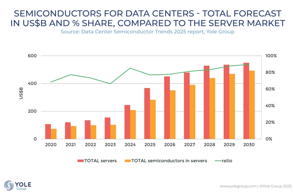
A $3 million grant from the U.S. National Science Foundation (NSF) to the University of Chicago aims to remove many of the challenges holding back the growth of American semiconductor and chip manufacturing and drive a skilled future workforce.
The NSF ACE-3D Chip Design Hub, awarded as part of The NSF Chip Design Hub program, will be centered at the University of Chicago and led by Farah Fahim, a CASE senior scientist at the UChicago Pritzker School of Molecular Engineering (UChicago PME) and Microelectronics Division Director at the Fermi National Accelerator Laboratory. The award will support the expansion of domestic talent pipelines, chip design ecosystems and industrial innovation with the goal of spearheading the next generation of semiconductor manufacturing in the U.S. UChicago and Fermilab staff scientists will collaborate on the UChicago-anchored ACE-3D.
“Here in the United States, we have very good chip design innovation, but it is not connected to the domestic manufacturing ecosystem,” Fahim said. “By giving academia access to advanced manufacturing resources, we can propel manufacturing efforts across the country.”
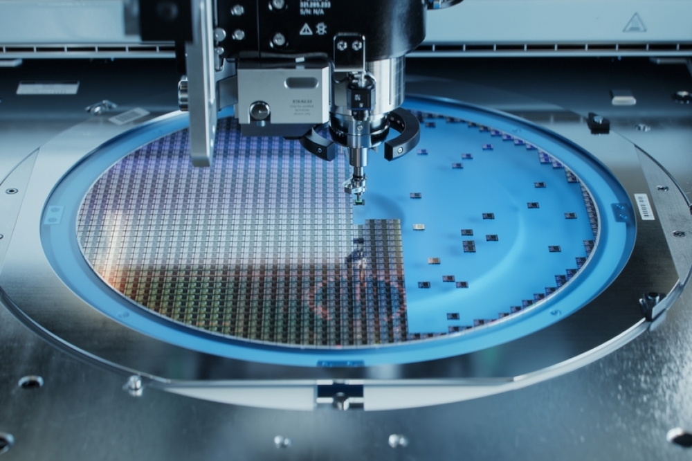
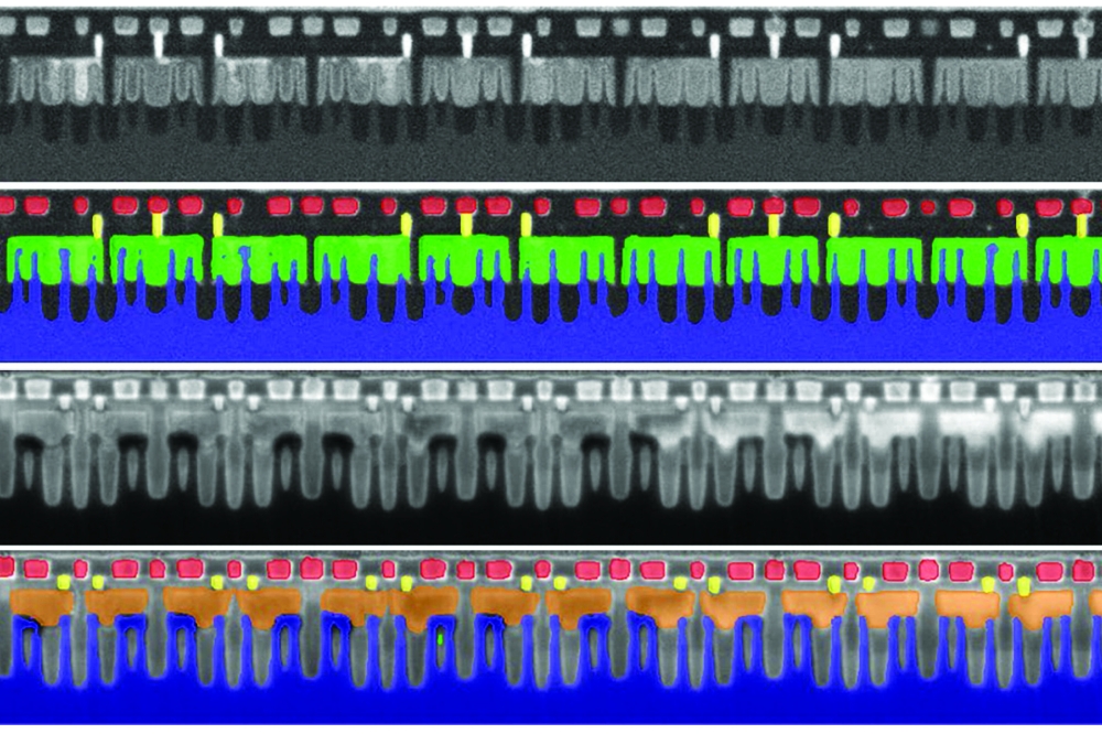
In addition to revolutionizing the design of vertically stacked chips, moving from the flat squares populating laptops and cellphones, the Advanced Chip Enablement (ACE-3D) Hub will focus on advanced 3D chip technologies, developing a user community and deploying new advanced technologies—creating practical, real-world tools to link academia, national labs and industry nationwide.
Previously, the needed manufacturing tools were disparate and hard to access. By combining tools into ready-to-go “design flows” and creating assembly design kits to show exactly how the complicated work is undertaken, Fahim hopes the country’s future workforce will find it easier to innovate in the domestic semiconductor space. The curricula and design flows that are being developed will be shared by ACE-3D with other academic institutions nationwide through this NSF program.
UChicago PME Dean Nadya Mason, who also serves as the University of Chicago’s Interim Vice President for Science, Innovation, and Partnerships, noted that ACE-3D will serve as a national resource both to advance science and technology and also to develop and train a skilled workforce to bolster U.S. innovation and economic competitiveness in 3D chip design.
“With our unmatched collaborations between academia, industry and national labs, UChicago is the natural place to grow both lab innovations and workforce solutions for the chip industry,” Mason said. “We are proud to be home to this new NSF center dedicated to spurring domestic semiconductor production.”
From help desks and design kits to tutorials and coursework, the goal is to remove the barriers between the undergrads, PhD students, postdocs and professors designing chips and the American manufacturers who will assemble them.
SHIELD USA (Substrate-based Heterogeneous Integration Enabling Leadership Demonstration for the USA) Program Director Jason Conrad said his group is excited to see the formation of UChicago ACE-3D. Led by Arizona State University in partnership with Deca Technologies, SHIELD USA was created in January to drive innovation in the domestic microchip packaging ecosystem, expand capacity for domestic advanced packaging and help regain U.S. leadership in microelectronics while strengthening national security.
“UChicago ACE-3D will fill critical gaps in knowledge and access to the latest electronic design automation tools and technologies that are essential for the US innovation leadership and workforce development,” Conrad said. “SHIELD USA looks forward to partnering with ACE-3D Hub to access and test our advanced organic substrates being developed as part of the NAPMP (National Advanced Packaging Manufacturing Program) project.”
Industry partners also said this new chip design hub will fill a major need in the market.
“We at NHanced are very excited to work with the University of Chicago ACE-3D Hub. The nation has a huge need for new talent that is trained to implement the next generation of semiconductor technologies,” said Robert Patti, CEO of manufacturer NHanced Semiconductors based in Batavia, Illinois. “As a manufacturer of 2.5D and 3D integrated circuits, and as a provider of a broad range of advanced semiconductor packaging, we see the ACE 3D Hub as vital for U.S. competitiveness.”
"The National Chip Design Hub and this award play a pivotal role in meeting the urgent need for a skilled semiconductor design and manufacturing workforce, particularly in the rapidly evolving field of 3D-IC and Heterogenous Integration," said Katy Crist, Director of Workforce Development at California-based Synopsys. "Synopsys is committed to powering innovation, and our Synopsys Academic & Research Alliances (SARA) furthers that vision by equipping over 200 American universities with the essential technology, training, and curriculum needed to empower the next generation of semiconductor innovators and leaders. Investments like this are crucial to sustaining United States' leadership in the dynamic semiconductor sector."
Co-principal investigators will include Northwestern University Prof. Seda Ogrenci, University of Illinois Urbana-Champaign Prof. Pavan Kumar Hanumolu, Arizona State University Prof. Hongbin Yu, University of Minnesota Prof. Yu Cao and UCLA Prof. Puneet Gupta.
The NSF Chip Design Hub program was created in 2023 to fund up to two Chip Design Hub awards. Purdue University’s Chipshub also has been recently selected for funding by the NSF.
Fahim described the two projects as highly complementary, with the Purdue hub providing foundational tools and curricula for chip design and the UChicago hub connecting the academic research community to advanced next-gen manufacturing processes.
“Manufacturing will thrive because chip design training will be more accessible and research will thrive because there will be a community supporting this important effort,” Fahim said.