Artificial intelligence in multimodal microscopy workflows for failure analysis: from 3D imaging to automated defect detection
Examining how the wealth of interconnected data will fuel the development of AI-based predictive models, capable of forecasting not only the occurrence but also the timing and underlying causes of failures from their earliest symptoms.
By Flavio Cognigni, Product and Application Sales Specialist XRM & Multimodal Microscopy and Heiko Stegmann, FIB-SEM application expert and advisor, Carl Zeiss Microscopy
Evolution of imaging technologies and the need for artificial intelligence in failure analysis
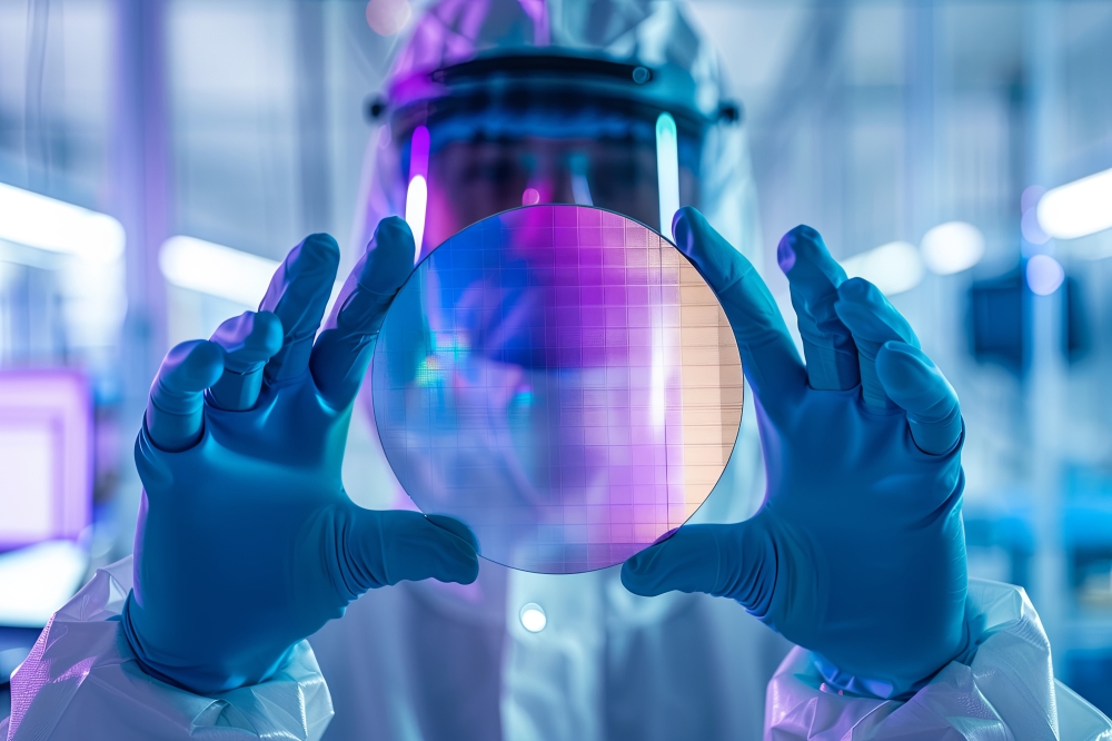
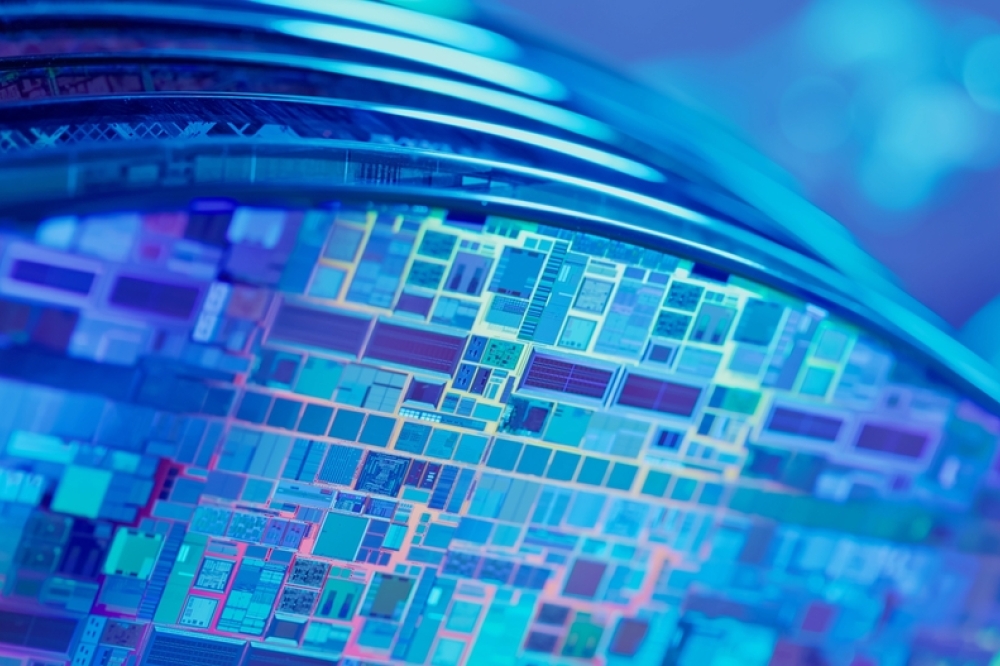
In the fast-evolving world of electronics and semiconductors, image processing and analysis have become essential pillars of innovation, reshaping failure analysis workflows. As devices have grown more compact, complex, and densely integrated, the demand for three-dimensional (3D), high-resolution, and non-destructive imaging has increased exponentially.
Image processing and analysis constitute a distinct field of research and application, drawing upon contributions from multiple scientific disciplines such as computer science, physics, mathematics, and engineering.
The integration of knowledge from these areas has significantly advanced our capabilities in enhancing, interpreting, and extracting meaningful information from complex image datasets, thereby enabling breakthroughs across a wide range of technological and industrial domains.
The increase in data volume, complexity, and dimensionality - particularly with the widespread adoption of 3D imaging and multimodal investigation workflows - has pushed traditional image analysis methods to their limits.
As a result, there is a growing need for smarter, more adaptive approaches capable of handling complex and large image datasets and automating repetitive analytical tasks.

Figure 1. U-Net Explained: Understanding its Image Segmentation Architecture, author: Conor O’Sullivan.
link: https://medium.com/data-science/u-net-explained-understanding-its-image-segmentation-architecture-56e4842e313a
In this article, we explore how artificial intelligence (AI) is transforming the way image data is processed and analyzed in the context of failure analysis (FA) for electronics and semiconductors. We highlight the core benefits of AI-based approaches, examine practical applications, and discuss the future implications for research, quality assurance, and industrial reliability.
Fundamentals of AI, machine learning, and deep learning in image analysis
To understand advancements in AI applied to image processing and analysis, it is important to define key concepts. AI broadly refers to computer systems that mimic human intelligence. Machine learning (ML) is a subset of AI, where computers learn from data without explicit programming. Deep learning (DL), a further subset of ML, uses neural networks - interconnected layers of nodes inspired by brain neurons - to process information.
Among neural networks, convolutional neural networks (CNNs) are the most commonly used in image processing. The U-Net architecture is particularly prominent in the field of image segmentation and analysis, known for its high performance even with limited training data, mainly due to the presence of skip connections that help preserve spatial information during feature extraction and reconstruction (Figure 1).
Advancing image reconstruction with DL techniques
The growing need for smarter, more adaptive approaches to manage increasing complexity and dimensionality has paved the way for AI to become a powerful ally in FA. By learning from data and adapting to context, DL models can overcome hardware limitations in image quality and throughput - enhancing 3D reconstructions, enabling the detection of finer, more complex structures and hidden features, and significantly improving both the speed and accuracy of data acquisition and interpretation (Figure 2a). DL-based models have found wide application in the field of super-resolution, where AI is used to transfer the fine pixel size of a high-resolution XRM scan - characterized by a small field of view (FOV) - to a lower-resolution scan that captures a larger FOV [1] (Figure 2b).

Figure 2. (a) Comparison between X-ray microscopy (XRM) datasets of a
modern graphics card, reconstructed using the traditional
Feldkamp-Davis-Kress (FDK) algorithm (left) and a DL algorithm (right).
DL reconstruction reveals fine details that are not visible in the
standard FDK reconstruction, as highlighted by the white arrows. (b)
Application of a DL-based super-resolution model to transfer the fine
pixel size of a high-resolution XRM scan (small FOV) onto a
lower-resolution scan capturing a larger FOV [1].
AI-powered image segmentation and its impact on semiconductor FA
Following reconstruction and initial image processing - such as filtering - image segmentation plays a critical role as the first and fundamental step in the image analysis pipeline. It involves partitioning an image into meaningful regions or objects, such as interconnects, vias, cracks, voids, or delamination which are essential for identifying defects and understanding failure mechanisms. The schematic shown in Figure 3 illustrates a general example of an image processing and analysis workflow.
Accurate segmentation allows for precise localization and quantification of structural features, enabling analysts to focus on areas of interest and extract relevant measurements. Traditional segmentation methods, such as histogram-based thresholding, are simple and, in several applications, may be a suitable solution for accessing and revealing the desired information contained in the dataset. However, the features and characteristics, as well as both the image analysis purpose and tasks, of certain images can limit the efficacy of these methods.
Without effective segmentation, downstream tasks such as defect classification, statistical analysis, or 3D objects visualization may suffer from reduced accuracy or interpretability. As device architecture becomes increasingly complex and image datasets grow in size, dimensionality and complexity, advanced segmentation - particularly AI-powered - is becoming indispensable for enabling scalable, consistent and reproducible FA.
Overcoming computational barriers: Cloud-based training for DL models
Performing image segmentation with DL models has opened new opportunities in FA. This approach requires model training, which involves dataset annotation and significant computational effort. To be practical, training must be completed within minutes - or at most, a few hours - using a limited number of images, as extremely large training datasets and long training times hinder real-world application (Figure 4).
The training phase is the most resource-intensive step. While local computing resources, such as high-power workstations, are often constrained by hardware limitations - CPUs, GPUs, memory, and storage - resulting in long processing times and limited scalability, cloud computing offers a flexible alternative [2].

Figure 3. AI-based workflow for image processing and analysis. The process includes dataset acquisition using the most appropriate characterization technique, AI-based denoising to enhance signal-to-noise ratio, object annotation for training segmentation models, automated dataset segmentation, and advanced quantitative analysis. Trained models can be reused for consistent and efficient analysis across similar datasets.
On-demand, pay-per-use platforms eliminate hardware barriers, provide elasticity to scale resources as needed, enable remote accessibility, and foster collaborative environments, all while reducing maintenance costs. These advantages make cloud solutions increasingly attractive for integrating DL into routine FA workflows.
Results reported in Figure 5 demonstrates how effectively DL models can segment noisy datasets - eliminating the need for extensive preprocessing - and images where different structures exhibit similar greyscale levels, making traditional methods such as histogram-based thresholding ineffective [3].
Building automated multimodal pipelines with DL and Correlative Microscopy
The entire AI-powered image processing and analysis workflow can be automated within compact, integrated multimodal pipelines that combine data analysis functional units, code integration, and data storage into a single software environment, enabling complex analyses and routine operations.

Figure 4. Using modern cloud-based software solutions for annotation, training, and segmentation, the development of customized DL models becomes possible with only a limited number of annotated images and objects. For illustrative purposes, three representative images are shown in the figure [2].
For example, a Superjunction MOSFET was investigated by combining FIB-SEM tomography with 3D energy-dispersive X-ray spectroscopy (EDX), integrating nanoscale morphological information with elemental mapping. The two datasets were aligned, and their combination enabled the training of a DL model capable of segmenting the entire dataset, capturing both morphological and elemental
features.
The case presented in [4] addressed a real-world industrial problem, demonstrating that this approach can automate the analysis of thousands of images from the same sample class (Figure 6).
AI algorithms can also be employed to reduce X-ray microscopy (XRM) scan time. Engineers have developed a multimodal characterization workflow that combines infrared imaging, multiscale XRM, and FIB-SEM tomography to investigate stealth laser dicing-induced defects in integrated radio frequency (RFID) devices [5].

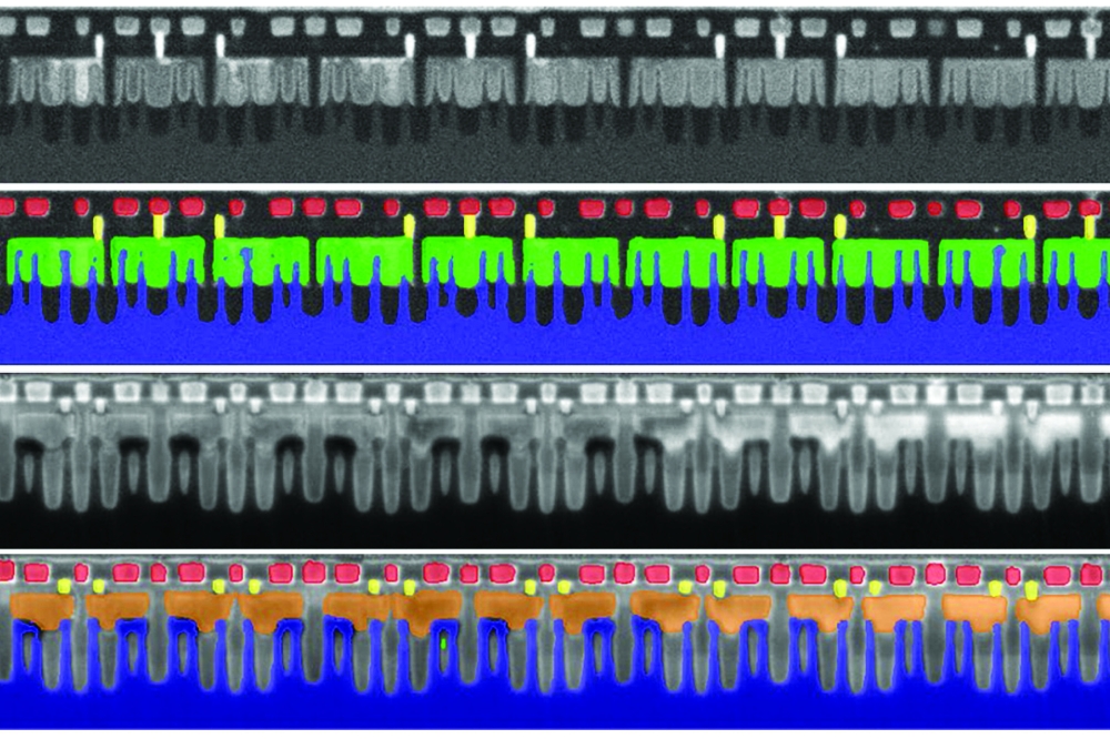
Figure 5. 2.45 x 0.29 µm2 sections of a (a) BSE and a (c) SE
images with their respective (b, d) segmentation with the following
color codes – blue: fins, green: gates, orange: SD, yellow: contacts,
red: M1 [3].
In this study, a 10x reduction in scan time was achieved while preserving the quality of the dataset, as reported in Figure 7a. A DL segmentation model enabled the visualization of a color-coded network of metal layers within the device, as depicted in Figure 7b.
A second DL algorithm was used to guide and streamline the identification of potential defect site locations within the FIB-SEM tomography dataset volumes of interest (VOIs). Engineers observed that defects could manifest
as low discharge between poly stripes and were often accompanied by small holes or voids within the first metal layer.
After two training cycles, the model demonstrated its ability to precisely identify these voids and holes, which may indicate the potential presence of a root cause of failure. Results are reported in Figure 7c,d.

Figure 6. Example of an AI-powered integrated workflow for failure
analysis. A Superjunction MOSFET was analyzed by combining FIB-SEM
tomography and 3D EDX, enabling the alignment of morphological and
elemental datasets. A DL model was trained on the combined data to
segment structures based on both morphology and composition, allowing
automated analysis across thousands of images from the same sample
class. This approach demonstrates the power of multimodal data
integration in real-world industrial applications [4].
The role of data management systems and AI in the connected laboratory of the future
As FA laboratories evolve, the implementation of robust data management systems (DMS) becomes critical for handling the large amount of data generated by multimodal characterization platforms. A DMS provides centralized storage, organization, and accessibility, enabling integration with AI-powered image processing and analysis workflows.

Figure 7 – (a) The reconstruction obtained using a DL reconstruction
algorithm (right) allowed failure analyst to obtain XRM datasets in ~ 20
minutes, whilst the standard FDK reconstruction (left) required ~ 4
hours scan time. The standard FDK reconstruction (middle), obtained
acquiring 161 projections, shows the typical radial artifact lines
related to missing angle information. These artifacts are avoided using
DL, while maintaining 161 projections, i.e., reducing the scan time by a
factor of 10 [5].
In the connected laboratory of the future, where instruments operate remotely and collaboration extends beyond physical boundaries, DMS platforms combined with multimodal microscopy and AI technologies will be essential.
They ensure efficient data management, support FAIR principles - at least within their own organizations - and accelerate the training of AI models for automated defect detection, thereby enhancing throughput, reproducibility, and innovation across semiconductor and electronics failure analysis [6].
Looking ahead, we foresee that the wealth of interconnected data will fuel the development of AI-based predictive models, capable of forecasting not only the occurrence but also the timing and underlying causes of failures
from their earliest symptoms. By dramatically reducing time-to-result and empowering us to design more resilient and intelligent devices, these advances will open a new chapter for humankind - one where our technologies harmonize with the delicate systems of our world, propelling us forward while carefully minimizing our footprint on the Earth.
For More Information
ZEISS Microscopy: www.zeiss.com/ai-multimodal-workflows