Material science innovations for advanced packaging applications
Wayne Rickard, Terecircuits CEO, outlines the company’s decision to join the US’s National Semiconductor Technology Center, contributing its considerable expertise in the synthesis, characterization and delivery of polymers, encapsulants and thin film coatings for advanced packaging. Wayne explains that, in working alongside industry leaders across the U.S. semiconductor ecosystem, Terecircuits can accelerate the development of advanced material solutions for heterogeneous integration and, in so doing, is helping to tackle critical challenges in high-density, high-performance chip manufacturing.
SIS: It would be great if we can start with a little bit of background, a brief introduction to the company?
WR: Sure. Terecircuits was actually founded by Dr. Jaina Sheets, and we got our first funding in 2019. She was driven by the vision that, eventually, advanced packaging would become a driver of advancements in semiconductor manufacturing and processing to complement Moore’s Law, and that when that happened, it would require new materials as well. As a physical chemist with a background of 20 years at HP Labs and a background in photolithography, Jaina was uniquely qualified to understand how that market might emerge.
SIS: You’ve recently joined the National Semiconductor Technology Centre (NSTC). It would be good to understand a bit about why joining is important, the benefits you expect to get and also what you will contribute?
WR: The National Semiconductor Technology Centre is an opportunity for a small company like us. As I mentioned, we’re a startup. We have less than a dozen employees. In material science, you’re only a small part of a larger ecosystem. Obviously, advanced packaging involves tool makers, it involves the ODMs, it involves the OSATs. Every part of the supply chain, every part of the interrelated infrastructure that’s required to build a semiconductor has unique requirements. Without having the ability to go out and buy and purchase the entire tool chain that you need to build a semiconductor, having something like this technology centre gives us the opportunity to interact with our peers and with the people that own and control the upstream and downstream processes, which is critically important as a material provider.
Then a secondary benefit is it’s very expensive as a material company to go out and qualify our material in different environments. Again, this brings everybody together under one roof where we can all interrelate and work on some of the problems the industry is facing together.
SIS: in terms of the technology portfolio you’ve got, I think that the sweet spot is around polymer chemistry. there’s a product solution called Terefilm and other things you do – please would you give us a bit more detail?
WR: Terefilm is a unique material. It combines some of the qualities of a temporary bonding and debonding, adhesive with the patternability of photolithography.
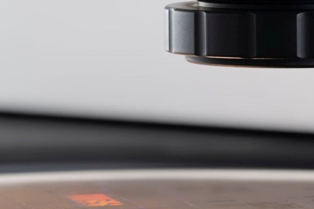
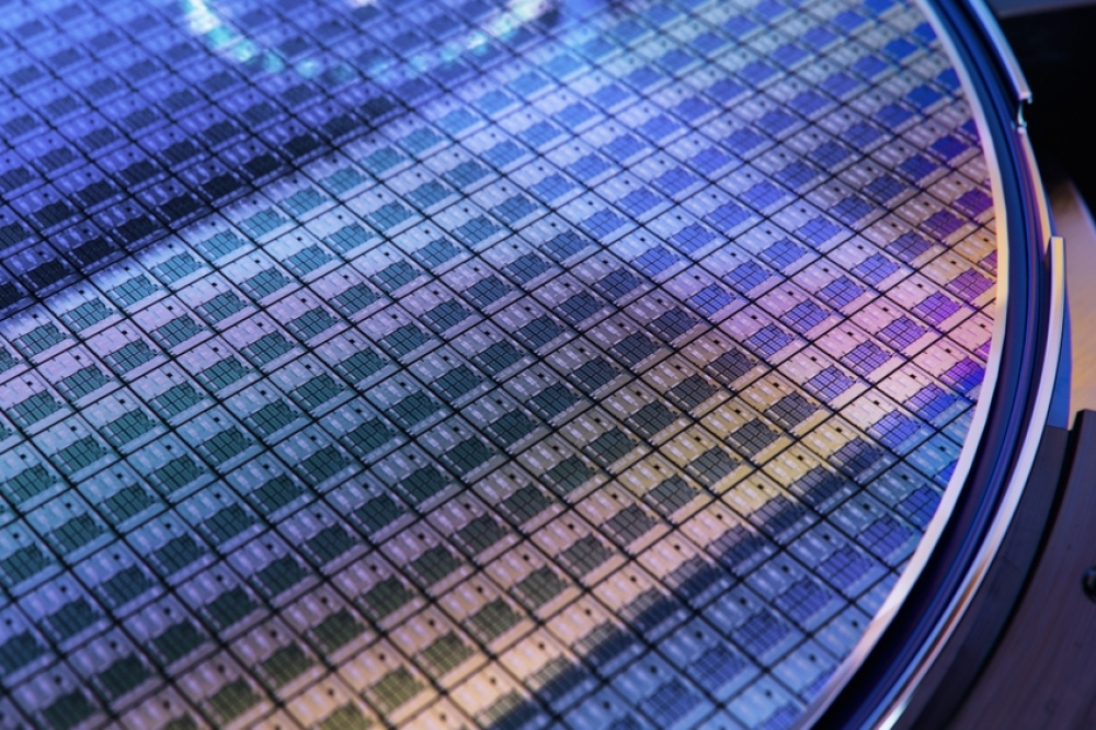
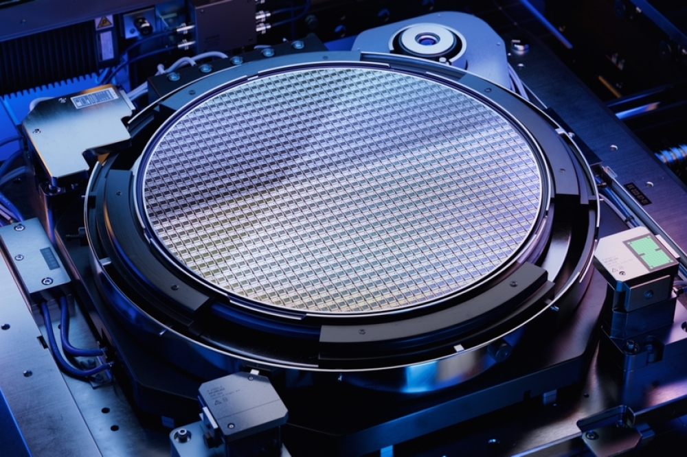
This is a very unique combination of characteristics. In temporary bonding and debonding, where you’re connecting two wafers together or chips to wafers, you have a release process that acts on the entire surface area of the bonding material. And that means it’s either bonded or it’s debonded. With lithography, though, you’re able to pattern an individual component. In the lithography, obviously, when we fabricate semiconductors, we’re doing that down at the nanoscale. But what we envisioned was a process where you could use a temporary bonding, debonding adhesive, and then pattern individual components that are being held by that adhesive, and then release them in a controlled way. And what that lets us do are some very unique things. It lets us handle material for one that is very, very small. So one example is micro-LEDs, which can be about the size of a grain of pollen. Very difficult for a pick-and-place tool, you can imagine, or something with a vacuum head to pick up something on the scale of a red blood cell.
But we can do that with our material. We can pick up an entire EPI wafer of components, and then we can target the ones we want to release. Just using a little bit of light and heating, we can target the ones that we want to release and place them on a substrate. This gives us the ability to handle things that are very small, but we can also handle components that are very fragile. An example might be something like silicon carbide or gallium nitride.
These materials are much more brittle than silicon, and conventional handling techniques can actually damage them. Our material can hold these components securely and then release them accurately at the point that you want to place them on a substrate. And then the final use case is for materials that are also very fragile, like a thin silicon wafer. When it’s silicon, the silicon is normally pretty rigid and easy to handle, but when it’s thinned down to under 50 microns, now it becomes much more fragile and difficult to handle. Again, our material can act as a temporary bonding, debonding adhesive and hold that material securely until you’re ready to release it and place it.
SIS: In terms of where you are, is that solution readily available for partners and others? Or is it still in test phase? What’s going on there?
WR: We’re sampling the material today. We have several partners that are evaluating the material for all three of the use cases I just mentioned, micro-LEDs for advanced display fabrication, for silicon carbide handling for die attach, and for thin wafer handling. All those use cases are actually being applied at various partners today. We also partner with tool companies. We’re, as I said earlier, a material company, so our expertise is in the polymer chemistry side of the equation. We still need to work with tool partners in the case of micro-LED placement, for example, that requires a laser placement tool. There are several companies that are involved in the development of these tools, and we work with them.
SIS: You also have expertise and innovation around lithography and process engineering. Is this ‘incidental’ to your main expertise, polymer chemistry, or are those separate major focuses or only in so far as they impact on the polymer chemistry that’s your sweet spot?
WR: That’s a good question. These are very complementary skill sets to have. If you develop advanced materials, particularly for advanced packaging, which is a fast evolving sector in semiconductor manufacturing, you need to have exposure to the complementary skills that are involved in bringing that material to market. For example, I mentioned that to pattern our material, you need to have a tool very much like a lithography tool. For us to even demonstrate our material, we’ve had to develop expertise in optics and in fine positioning systems. This requires some mechanical engineering expertise. This is not to say that we want to be in the tool business, but to attract the tool companies to what our process is capable of, we need to demonstrate the material. We’ve actually built lab-scale tools that can do everything I’ve described, place components with micron accuracy on a substrate and release individual components with one micron between them. This is the type of thing that if you don’t see it demonstrated, it’s difficult to believe it’s even possible. Again, process engineering skills, lithography skills, and skills in optics and lasers are all complementary skills we’ve had to develop.
SIS: Without labouring the point, bearing in mind this expertise you have developed, is this something you think might turn into an opportunity - whether you just licence someone to produce these tools or is it just a means to an end, and once the polymer chemistries and Terefilms out there, you will no longer have a need to develop these tools?
WR: That’s a good question. I think from our standpoint, we want to enable as many tool vendors as possible to use a material like ours. It’s good for the industry, and each of the verticals that I’ve described is probably going to have some nuance in the tool design. If you’ve ever talked to a tool vendor, in a perfect world, they’d build one tool and it would work for everybody. But the reality is there’s a nuance to every deployment that requires the tool to be tweaked a little bit and optimised for the individual process flow. By working with a lot of tool vendors and helping them tune in their process with whatever the process parameters are that need to be adjusted, we can attack multiple verticals in parallel. The tool vendor partner for display technology is going to be very different than the tool vendor that’s focused on power semiconductors.
SIS: You’ve referenced a couple of times advanced packaging, which is the end goal. As you said, it’s fast moving. Your thoughts more generally as to the challenges and opportunities in terms of where you’re at and the potential you see for yourselves within this exciting area would be great to understand?
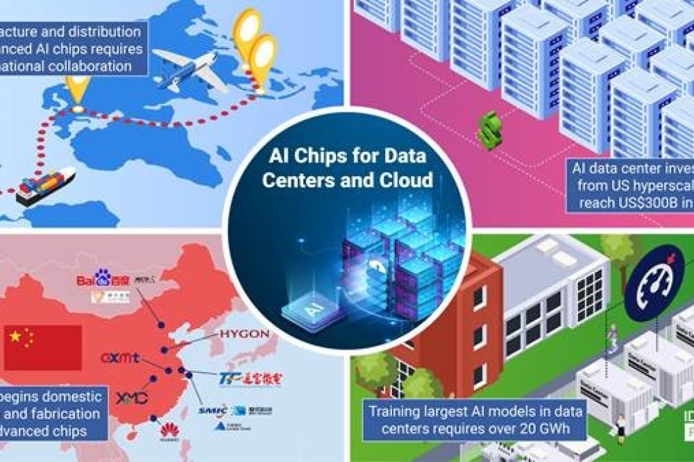
WR: Advanced packaging is indeed a fast moving, fast evolving area. And today, at the very peak of what’s capable in advanced packaging, it’s dominated by the large companies like Samsung and TSMC who have internal processes. Intel has a process. But to really get advanced packaging into the mainstream so that it can be adopted by the OSATs and so that we can drive the advanced packaging techniques down into the mainstream of semiconductor manufacturing for standard components, not just for the latest GPU from NVIDIA - this is something that’s going to require a lot of process optimisation. It’s going to require a lot of new materials.
It’s also going to require us to reimagine and reinvent some of the ways we assemble semiconductors today. When you think of advanced packaging, in the past, packaging involved one die on a substrate, wire bonded to a lead frame and encapsulated. Today, advanced packaging involves tens, or in some cases, hundreds - in the case of a micro-LED panel, millions of components that need to be assembled in some type of a larger assembly. This can involve things like co-packaged optics. It can involve thin film batteries, passives, different process nodes.
The latest process node that you use for the GPU, for example, is not the same process node that’s required for the memory. And that means that you’ve shifted from a problem that has been largely solved by integrating on a monolithic chip. Now you’re distributing that problem across multiple different components. Of course, one of innovations is chiplets, which are small building blocks that can be used to build more complex assemblies. But again, chiplets also create a packaging challenge because they have to be placed on a substrate with high accuracy, in some cases, very close to each other, in some cases, even stacked in the third dimension.
All of these challenges involve... and when we think about the tools we have to do that, we really have pick-and-place tools, which, as I mentioned earlier, get increasingly challenged as components get small, thin, and fragile. And you have flip-chip die bonders, this is a tool that does things one at a time, or maybe five or six at a time on a multi-head tool. This does not give you the throughput and the yield that is required to go from where you can afford to pay for very expensive tools to something that can be acquired by an OSAT.

SIS: In terms of the NSTC, you’ve explained the benefits of being part of a bigger collaborative organisation. Is this so important to you? The organisation’s goals include the US’s semiconductor industry, developing that and reducing the time from lab to fab. I guess what you’ve explained there, you’ve very much committed to that. But just in terms of the US semiconductor industry, are you keen to help that or do you regard yourself as part of the global semiconductor industry, if you like?
WR: I think we’re part of both. The challenges that the global industry is facing, the ones I mentioned about advanced packaging are common to the entire industry. As far as the US is concerned, the challenge the US has is, again, this push for independence of the supply chain is a consequence of increased specialisation across geographies. For example, the EDA tools and the design of semiconductors, this expertise is in the US. But when you get to lithography tools, some of the more advanced tools that are used in the process of manufacturing, Europe has a lot of the competency there.
Advanced materials, the competency is in Japan. And of course, packaging and assembly has traditionally been in Southeast Asia. This dispersion of competencies is something that makes the entire semiconductor industry more interdenpendent. I think what COVID taught us was that when supply chains are disrupted, you end up with a situation where for the lack of a semiconductor in a radio, you can’t build a car. And that really was a wake-up call for the industry to say we need, if not complete reshoring, we need less interdependence.
We also need to move some of our supply chain dependencies from regions that may be more impacted, either by geopolitical situations or by supply chain disruptions like COVID, to something where we’re less dependent on single points of failure.
That’s part of what the National Semiconductor Technology Centre is trying to do for the US, which is flatten the supply chain a little bit through this type of reshoring and bringing some industries that have traditionally been located in other geographies back into the US.
SIS: I was going to ask you about what I always call the three Ss. You’ve talked about the supply chain, but we’ve got skills, which everyone says there aren’t enough people to go around and it’s going to get worse. But as I always say, I don’t see anyone break into a sweat about it, but, potentially, it sounds like quite a large problem. Then there’s sustainability. There’s maybe a bit of pushback at the moment geopolitically, but I think the industry is, to a certain extent, on a path towards sustainability anyway. It would be good to have your thoughts as to these challenges?
WR: Skills and workforce development is something that comes up all the time - when you have allowed some core competency to go to a geography where they’ve developed the expertise over the last couple of decades, and you’ve allowed that skill set to atrophy domestically.
Now you find, if you really want to do some level of reshoring, that you don’t have the skilled workforce that’s required. It may be that it’s experiential because you haven’t been doing manufacturing in the US, or it may be that you don’t have the educational discipline in the institutions to do the type of job on preparing people for entering in the semiconductor field.
I see that changing a lot. Almost all the major organisations, like SEMI and even the individual companies that are involved in semiconductor manufacturing have workforce development programmes right now, outreach to universities, certificate programmes. It’s becoming something that, while I think it will continue to be a problem for a while as you try to bring resources to different regions that don’t have the base established, it’s something that the industry is addressing A good example is TSMC building fabs in Arizona. One of their critical concerns was, would we be able to find a skilled enough workforce outside of Taiwan to actually run them?
There were some fits and starts, but I think the evidence now is pointing to the fact that it is possible to build a skilled workforce in a region that hasn’t traditionally been part of the industry.
WR: Sustainability is something I think one of the areas that always comes up. I’m here in Arizona, and we always are asked about, what about if the centre of gravity for the US semiconductor industry is moving to Arizona, what about water? What you’ve seen in companies, I think Intel is a great example, is the ability to recycle a lot of the water that’s used in the semiconductor process so that you really aren’t using a lot of water.
You’re not consuming a lot of water, you’re reusing a lot of water. That’s a big development in sustainability in the processing of manufacturer’s semiconductors. This has happened in the last decade.
The other thing to remember about sustainability is that we’re moving to an era where this is the electrification era, where we’re looking at things like electrical vehicles, we’re looking at non-traditional sources of power like solar and wind power. All these sources of energy that will generate and consume electricity, they’re going to benefit from the transition from silicon to power semiconductors like silicon carbide and gallium nitride. I’ve seen statistics that say just by using silicon carbide in an electrical vehicle drivetrain instead of silicon for power conversion, you can get a 7% improvement in range in that electrical vehicle.
Because silicon carbide is more efficient, you’ll also get a lighter powertrain, which also adds to the efficiency. You’ll be able to eventually use higher voltages for charging stations. Power semiconductors will enable you to charge an electrical vehicle in the same amount of time it takes to fill a tank of gas, which is one of the last barriers to electrical vehicle adoption. All of this will drive less dependence on fossil fuels and more reliance on cleaner and more efficient sources of energy. A lot of that’s enabled by these new advances in semiconductors.
SIS: In terms of the industry’s future, obviously, we live in uncertain times, shall we say. In terms of the reshoring and the more insular approach that different countries, regions are taking, do you think that is going to damage the industry to a worrying extent, or is it something the industry can adjust to? Because as you explained eloquently a few minutes ago, each region of the globe has expertise in certain areas, and altogether, as a global industry, it’s fantastic. If each country or region has to start becoming more self-sufficient for that whole supply chain, there might be opportunities, but also challenges?
WR: Right. You mentioned the three S’s, and I think there’s also the three R’s, which are resiliency, which we talked about, reshoring, which we talked about, and R&D, which is the third leg, which is where we’ve all fallen behind
is in area. My company is a great example. The US is not really known for having a centre of competency
in advanced materials for semiconductors. That’s largely concentrated in Japan.
As we focus on closing the gaps that we have domestically, whether it’s materials or whether it’s packaging and assembly, as we focus on closing those gaps, and as other regions like Europe, and they have their own version of the Chips Act, as they focus on closing their own gaps and get better at chip design and EDA tools, we all end up becoming more competent, we become more competitive globally.
The fact is that we’re never going to be 100% completely onshore. The supply chains are too interrelated and too complicated. The best we can do is hope to have strong partnerships with aligned communities of interest to avoid some of the geopolitical stress. But once we’ve done that, the fact that we’ve all tried to close these gaps in our own ability means that we’re all stronger together.
I think that’s a very positive sign for the future the industry.
SIS: Maybe just finally, in terms of the company, Terecircuits, anything you can share on the company’s roadmap?
WR: Sure. Well, of course, Terefilm is our flagship product, and it has use cases across many aspects of advanced packaging assembly for precision placement and as a way to replace in some extreme cases what we can’t do with pick-and-place tools.
There’s lots of work still to do building up that product category and bringing more tool players into that world.
For Terecircuits beyond that, we have an IP portfolio that’s fairly deep, and it includes other materials like encapsulants. We’re doing some work with materials that have a negative coefficient of thermal expansion.
By using those as doping agents in traditional encapsulants and underfills, you can actually make a material that has better heat transfer characteristics because now you’re not needing to load it with as much silica.
This is an area of investigation for us. We also are doing works with photoimageable masks, we’re doing this with liquid metal amalgams. We have quite a dense portfolio of IP that we haven’t even begun to exploit yet. Our plate is quite full with the one material that we’re taking to market now!