Thermal Management for Advanced Semiconductor Packaging 2026-2036: Technologies, Markets, and Opportunities
Ten-year TIM1/TIM1.5 forecast for advanced semiconductor packaging (ASP) split by graphene, liquid metal, thermal gel, and indium foil. 10-year forecast for microfluidic cooling. Detailed analysis on thermal and power management for ASP.
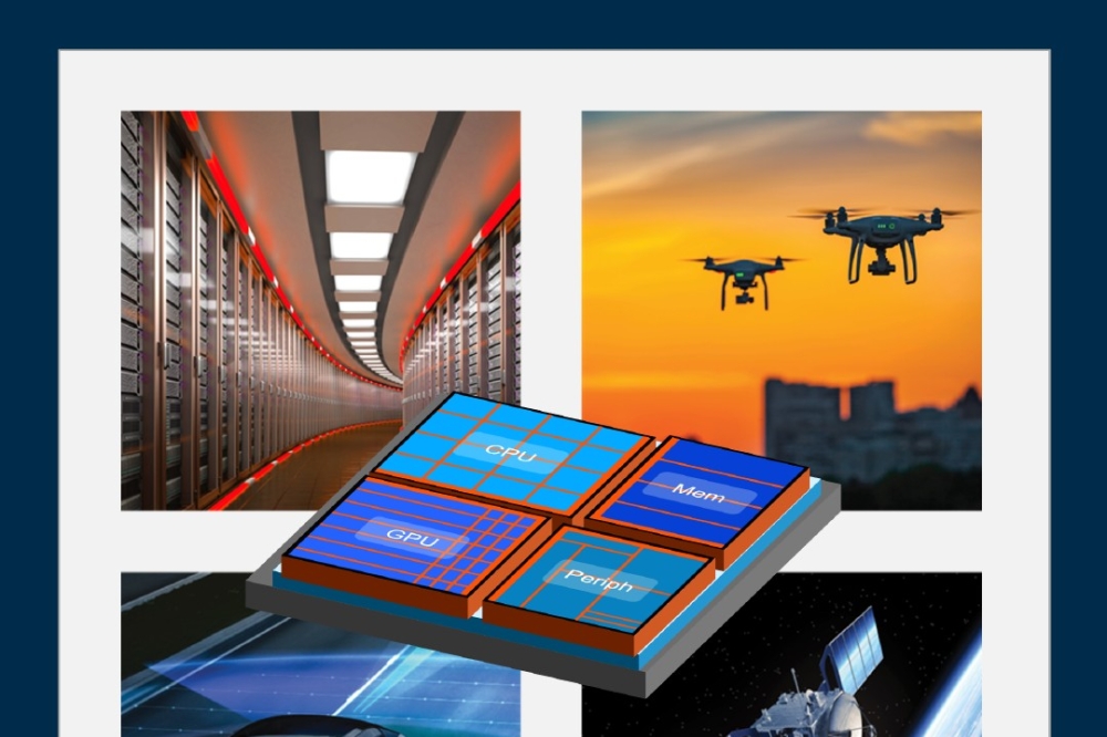
As AI computing demands and the thermal design power (TDP) of high-performance chips continue to rise, and the industry shifts from 2.5D to 3D packaging architectures, thermal management has emerged as a key barrier to large-scale commercialization and adoption. To address this growing challenge, the industry is exploring a range of strategies, including the use of advanced thermal materials (such as liquid metal, diamond, and graphene), lidless chip designs, optimization of the power delivery network, implementation of backside power delivery, and the adoption of liquid and microfluidic cooling technologies.
The IDTechEx report, "Thermal Management for Advanced Semiconductor Packaging 2026-2036: Technologies, Markets, and Opportunities", provides a comprehensive analysis of the transition from 2.5D to 3D advanced semiconductor packaging (ASP), advancements in power delivery methods (e.g., backside power and through-silicon vias), thermal challenges associated with 3D integrated circuit packaging, the use of innovative thermal materials (such as thermal interface materials and diamond substrates), and the implementation of liquid cooling techniques, including direct-to-chip, immersion, and microfluidic cooling systems.
Key contents from the report include:
A 10-year area forecast for TIM1 and TIM1.5 for advanced semiconductor packaging, segmented by material type including liquid metal, graphene sheet, indium foil, and thermal gel
A 10-year market size forecast for TIM1 and TIM1.5 for advanced semiconductor packaging, segmented by these materials
A 10-year volume forecast for microfluidic cooled advanced semiconductor packaging units
A 10-year market size forecast for liquid cooling for high-end data center semiconductors, segmented by direct-to-chip/cold plate and immersion
Thermal management challenges for 2.5D and 3D semiconductor packaging
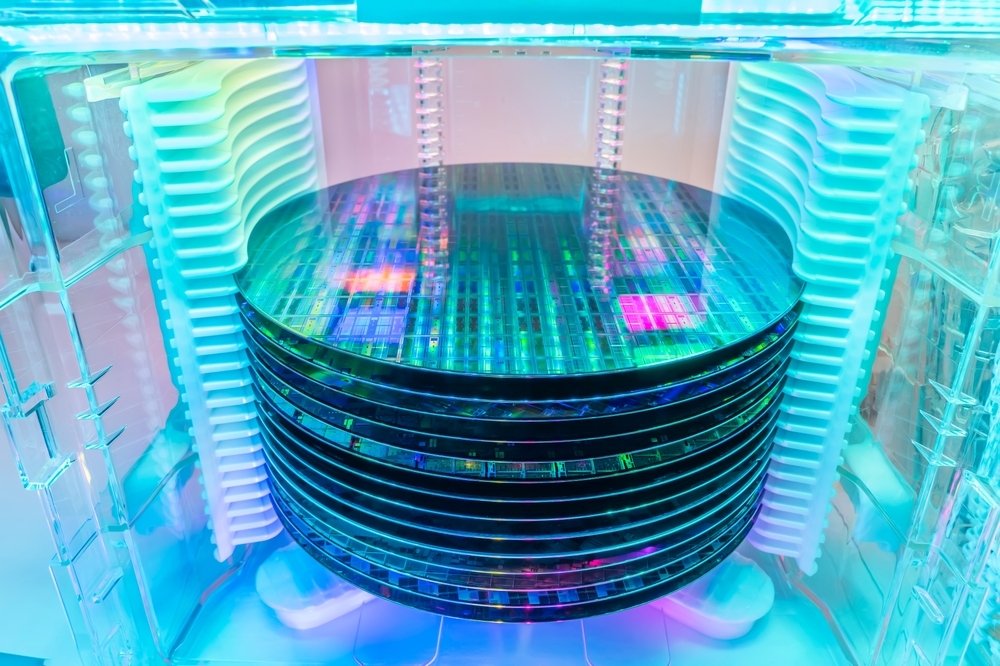
As of 2025, 2.5D semiconductor packaging, such as TSMC's CoWoS technology, remains the dominant approach for high-performance chips like the B200. To push performance further, particularly in terms of bandwidth and latency, the industry is increasingly focusing on a shift toward 3D packaging. Unlike 2.5D architectures, where the logic die and vertically stacked high-bandwidth memory (HBM) are placed side-by-side on a shared interposer, 3D packaging involves stacking an active die directly on top of another active die. This vertical integration, while promising for performance gains, introduces significantly greater power and thermal management challenges.
Power Challenges in 3D ICs
In 3D ICs, power delivery becomes significantly more complex than in 2D due to increased current density, limited pin access, and the use of vertical interconnects. A k-tier 3D stack draws approximately k times the current of a 2D chip with the same footprint, but power pins and packaging resources do not scale accordingly. This imbalance leads to multiple challenges. TSVs used in power delivery introduce substantial resistance, typically around 1 Ω per stack, resulting in greater IR drop and difficulty maintaining a stable supply voltage. Power is typically delivered through the bottom tier, which must carry the cumulative current for the entire stack, making it especially vulnerable to voltage droop and dynamic noise. This is further complicated by the fact that power-hungry compute blocks are often located near the heat sink, also on the bottom tier. Meanwhile, effective decoupling is hindered by limited white space, as TSVs and dense routing reduce the area available for placing decoupling capacitors. These combined effects worsen voltage fluctuation across the stack, increasing performance variability, timing uncertainty, and reliability risks, especially under peak-load conditions.
Thermal Challenges in 3D ICs
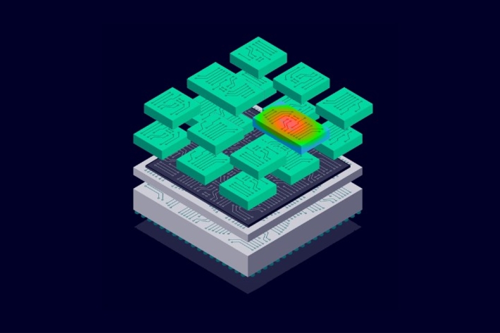
Thermal management is one of the most critical bottlenecks in 3D ICs. Unlike 2D designs where heat dissipates laterally and upward toward the heat sink, 3D stacks consist of thinner dies that limit lateral heat spreading. In addition, the middle dies are prone to heat accumulation, as they are farther from the heat sink and have limited effective thermal escape paths. Moreover, the vertical heat removal path is limited by the low thermal conductivity of inter-die materials such as dielectric layers and bonding adhesives. This leads to thermal hotspots that degrade performance and reduce reliability due to increased leakage and stress on interconnects. Another key issue is the close proximity of high-power logic blocks and memory can result in significant thermal coupling between tiers, further complicating thermal design. Conventional cooling methods often fail to reach the buried layers effectively, making it necessary to consider alternative techniques such as thermal TSVs and chip-level microfluidic cooling. However, these methods introduce their own trade-offs in terms of design complexity, cost, and integration challenges.
Materials innovations for more efficient heat transfer
To support more efficient thermal management in both 2.5D and 3D semiconductor packaging, the industry is actively exploring several innovative solutions. One key area of focus is the development of advanced thermal interface materials (TIMs). The IDTechEx report, "Thermal Management for Advanced Semiconductor Packaging 2026-2036: Technologies, Markets, and Opportunities", offers a detailed analysis of TIM technologies, particularly TIM1 and the emerging TIM1.5 category. These materials include options such as liquid metal, indium foil, graphene sheets, and next-generation thermal gels with enhanced thermal conductivity.
As of 2025, Shin-Etsu's X23 remains a widely adopted TIM1 material for ball grid array (BGA) applications. However, with rising thermal design power in advanced chips, the industry is increasingly turning to novel TIM1 and TIM1.5 materials that offer higher performance. Promising candidates include liquid metal, graphene-based materials, and thermal gels infused with highly conductive fillers.
In parallel, there is a shift away from the traditional two-layer TIM structure (TIM1 and TIM2) toward a single TIM1.5 layer. This approach aims to reduce thermal resistance by minimizing material interfaces. While this may reduce the number of TIM layers used, it does not necessarily shrink the overall market, as TIM1.5 materials tend to command higher unit costs due to their demanding technical specifications. IDTechEx forecasts that the combined market for TIM1 and TIM1.5 will grow to approximately US$500 million by 2036, highlighting a substantial commercial opportunity.
Beyond TIMs, another promising area of research is the use of diamond, particularly copper-plated diamond, as a substrate material for high-end semiconductor packaging. The IDTechEx report also delves into the latest developments, technical challenges, and future prospects surrounding the integration of diamond substrates into advanced packaging architectures.
Liquid cooling, immersion cooling and microfluidic cooling
Beyond material innovations, active liquid cooling is becoming an increasingly important trend in advanced thermal management. In high-performance data centers, technologies such as direct-to-chip and immersion cooling have already reached commercial deployment. Notably, the adoption of cold plate cooling in Nvidia's GB200 and NVLink72 configurations in the previous year has further solidified its position as the dominant near-term solution. IDTechEx expects cold plate cooling to remain the leading approach for at least the next 2-3 years.
However, both cold plate and immersion cooling primarily address heat dissipation from the chip package to the ambient environment. The more pressing thermal challenge lies within the packaging itself—specifically, managing the heat generated between vertically stacked components in 3D packaging architectures. To date, the industry has yet to establish a clear solution for this issue.
IDTechEx identifies microfluidic cooling as a promising candidate for addressing this internal thermal bottleneck, despite the complexity involved in its implementation. Microfluidic cooling uses intricate networks of microchannels to circulate liquid coolant either within the package lid or directly inside the packaging structure. While various architectural configurations are under development, the technology still faces several hurdles, including high design and manufacturing complexity, concerns about scalability, and limited data on long-term reliability.
The IDTechEx report provides an in-depth analysis of ongoing R&D efforts in microfluidic cooling and outlines potential architectural roadmaps for its future adoption in advanced semiconductor packaging.
Conclusion
With the transition to 3D packaging for higher bandwidth and efficiency, multiple solutions (e.g., backside power delivery, integrated voltage regulator, advanced TIM1s, microfluidic cooling, etc.) have been proposed and investigated to address the thermal challenges. As of mid 2025, there are still significant challenges such as the trade-off between TSV density, manufacturing complexity, and defect rate, the balance between microfluidic cooling and commercial scalability. Therefore, industry players are making significant efforts to resolve these issues, and IDTechEx's report "Thermal Management for Advanced Semiconductor Packaging 2026-2036: Technologies, Markets, and Opportunities" provides a comprehensive overview of potential packaging architecture innovations, novel materials and active cooling strategies, as well as the projected market growth of different technologies over the next 10 years.
Key Aspects
This report provides critical market intelligence on the power and thermal management challenges of advanced semiconductor packaging (2.5D and 3D), novel thermal materials, and the trend of liquid cooling solutions.
This includes:
An overview of the 2.5D and 3D semiconductor packaging structure
An overview of thermal challenges in 2.5D and 3D packaging and integrated circuits.
Power management in 2.5D and 3DIC, including introduction to Power Delivery in in Advanced Semiconductor Packaging for HPC, Power Delivery Network (PDN) Evaluation of 2.5D, Power Delivery Network (PDN) Evaluation of 3D, and case studies from Industry Players
A comprehensive analysis of different cooling technologies for chips, including direct-to-chip cooling and immersion cooling, with cost analysis.
A review of novel thermal materials for 2.5D and 3D packaging, including liquid metal, indium foil, graphene sheet, and silver-filled thermal gel. Roadmap analysis of emerging TIM1 and TIM1.5.
Overview and analysis of diamonds for advanced semiconductor packaging, including diamond as a substrate and diamond as an interposer.
Area and market size forecasts from 2026-2036 for TIM1 and TIM1.5 for advanced semiconductor packaging, split by liquid metal, indium foil, graphene sheet, and thermal gels.
Unit forecast from 2026-2036 for advanced semiconductor packaging units with microfluidic cooling.