AGI Infinity reveals patent‑ready optical architecture

Independent assessment suggests the invention may represent a new direction in compute and interconnect architecture, positioning the company at what it describes as a “once‑in‑a‑generation inflection point” for future AI infrastructure.
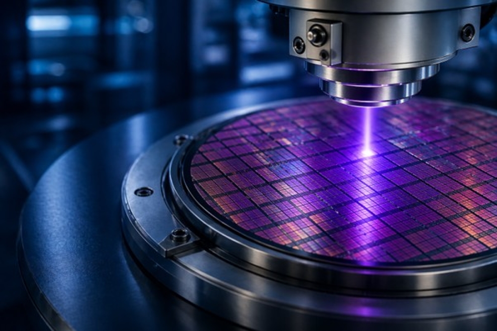
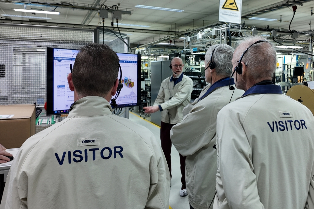
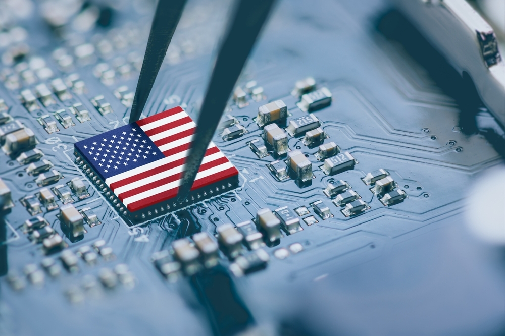
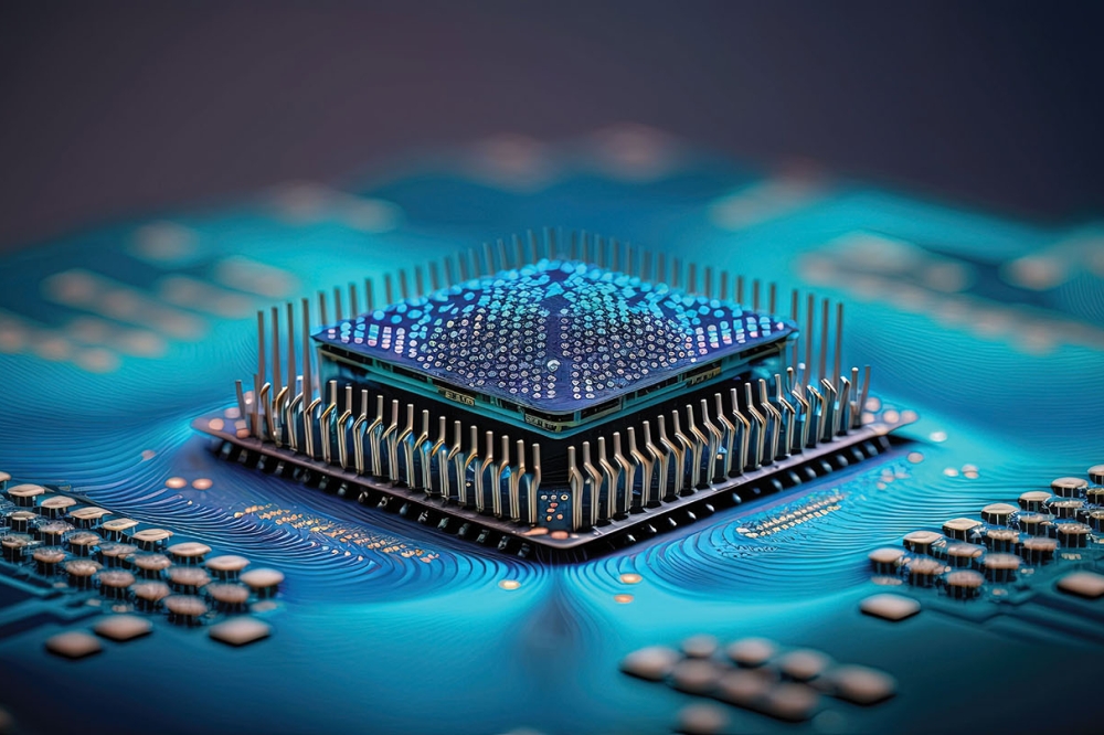
AI systems are scaling at extraordinary speed, but the hardware beneath them is struggling to keep pace. As workloads grow, the cost of moving data - bandwidth limits, heat, energy consumption, routing complexity and cooling overhead - has become one of the most significant constraints in modern computing. These pressures are already contributing to global chip shortages, rising data‑centre operating costs, and architectural bottlenecks across AI accelerators, HPC systems and cloud infrastructure.
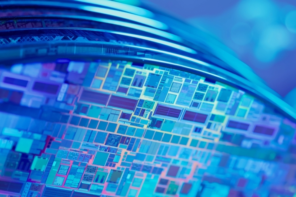
AGI Infinity’s ‘Wires to Waves’ platform is being developed to investigate whether volumetric holographic optical structures can provide a practical route to higher‑bandwidth, lower‑loss data movement - and, over time, new forms of optical switching and logic behaviour. The company’s patent centres on two core elements: Holographic Optical Conductors (HOC), designed to provide optical alternatives to selected electrical interconnects, and Holographic Optical Transistors (HOT), transistor‑like optical structures intended to enable switching and logic behaviour within holographically structured materials.
Following a major technical update, AGI Infinity has now completed two simulations validating the core patent claims, demonstrating that both the micro‑scale and nano‑scale elements of the architecture can operate within a single, fully volumetric 3‑D construct. This has allowed the company to unify its development work into one hybrid platform, integrating earlier micro‑scale pathways with the nano‑scale NANNI‑O concepts into a cohesive architecture designed for real‑world semiconductor environments.
The unified architecture is intended to explore whether structured light, guided through volumetric holographic media, can support higher‑bandwidth, lower‑latency data movement, reduced resistive losses, improved thermal characteristics, simplified routing in dense compute environments, and new optical switching concepts relevant to future AI hardware. The company emphasises that this is not a claim of full semiconductor replacement, but a focused exploration of whether a new medium for signal transport and switching can complement, integrate with, or eventually extend beyond conventional CMOS environments.
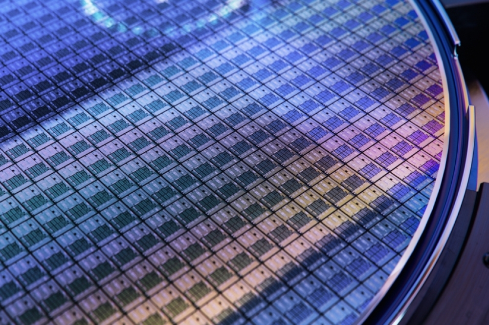
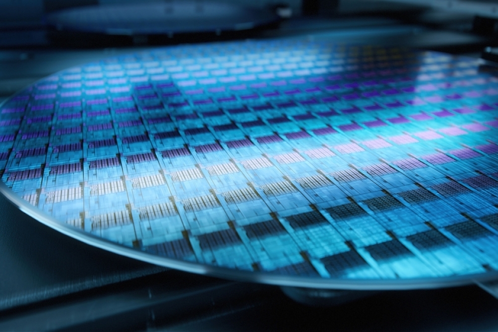
Deloitte forecasts the global semiconductor market will reach US$975B–$1T by 2026, driven heavily by AI‑related demand. As power, cooling and interconnect efficiency become first‑order design constraints, AGI Infinity believes the industry is entering a structural transition comparable to the move from planar transistors to 3D stacking. The company’s patent now reflects this shift, incorporating claim families around Z‑axis stacking, multiplexed addressing, chiplet/interposer embodiments, calibration, redundancy and self‑healing - features that align with the IEEE Heterogeneous Integration Roadmap and current industry pain points.
AGI Infinity believes this direction is commercially significant because it addresses challenges that are both technical and economic. As AI infrastructure expands, the industry faces mounting pressure to improve system efficiency, reduce energy and cooling demand, and unlock greater throughput from increasingly complex hardware environments. If validated, AGI Infinity’s approach could be relevant to semiconductor manufacturers, AI accelerator companies, high‑performance computing environments, advanced data‑centre systems, optical routing and packaging applications, and organisations exploring post‑CMOS infrastructure.
“Meaningful adoption won’t happen overnight,” the founders said. “But the industry is already moving toward chiplets, advanced packaging and co‑packaged optics. Our work is aimed directly at those bottlenecks. The transition from wires to waves will define the next era of AI.”