
Applied Materials Unveils eBeam Metrology System
Applied Materials has unveiled a unique eBeam metrology system that enables a new playbook for patterning control based on massive on-device, across-wafer and through-layer measurements.
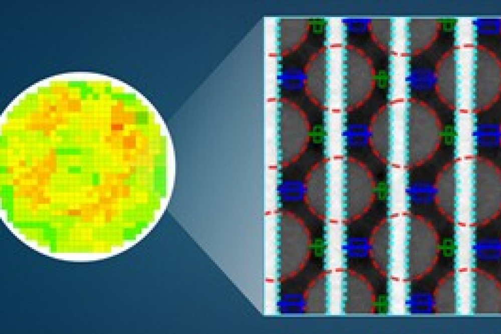
Advanced chips are built one layer at a time, and each of billions of individual features must be perfectly patterned and aligned to create working transistors and interconnects with optimal electrical characteristics. As the industry increasingly moves from simple 2D designs to more aggressive multipatterning and 3D designs, a commensurate breakthrough in metrology is needed to perfect each critical layer and enable the best performance, power, area-cost and time to market (PPACt).
Traditionally, patterning control has been achieved using optical overlay tools that help align die patterns with “proxy targets” which are guide marks printed into the spaces between die that are removed from the wafer during die singulation. Proxy target approximation has been complemented with statistical sampling of a small number of die patterns from across the wafer.
However, after successive generations of feature shrinking, broader adoption of multipatterning, and the introduction of 3D designs that cause interlayer distortions, the traditional approach is leading to measurement deficiencies – or “blind spots” – that are making it more difficult for engineers to correlate intended patterns with on-die results.
With the arrival of new eBeam system technology that can directly measure semiconductor device structures across the wafer and through layers at high speed, customers are moving to a new patterning control playbook based on big data. Applied’s latest eBeam metrology innovation – the PROVision 3E system – is especially designed for this new playbook.
“As the leader in eBeam technology, Applied Materials is giving our customers a new playbook for patterning control that is optimized for the most advanced logic and memory chips,” said Keith Wells, Group Vice President and General Manager, Imaging and Process Control at Applied Materials. “The resolution and speed of the PROVision 3E system allows it to see beyond the blind spots of optical metrology, performing accurate measurements across the wafer and between the many layers of a chip. This provides chipmakers with the multidimensional data sets they need to improve PPAC and accelerate the time to market of new process technologies and chips.”


