Ireland begins high-volume production of Intel 4 Technology

Intel deploys extreme ultraviolet lithography in high-volume manufacturing; use of the technology in Ireland is a first for mass production in Europe.
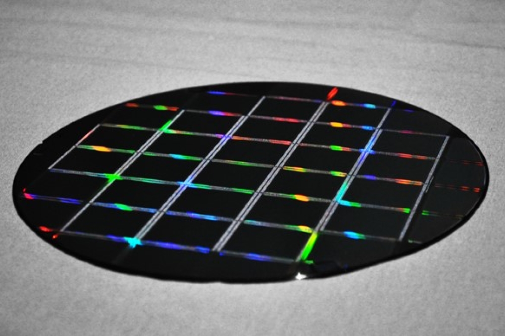
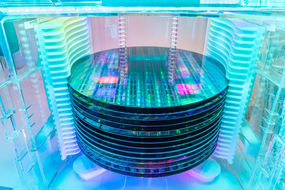
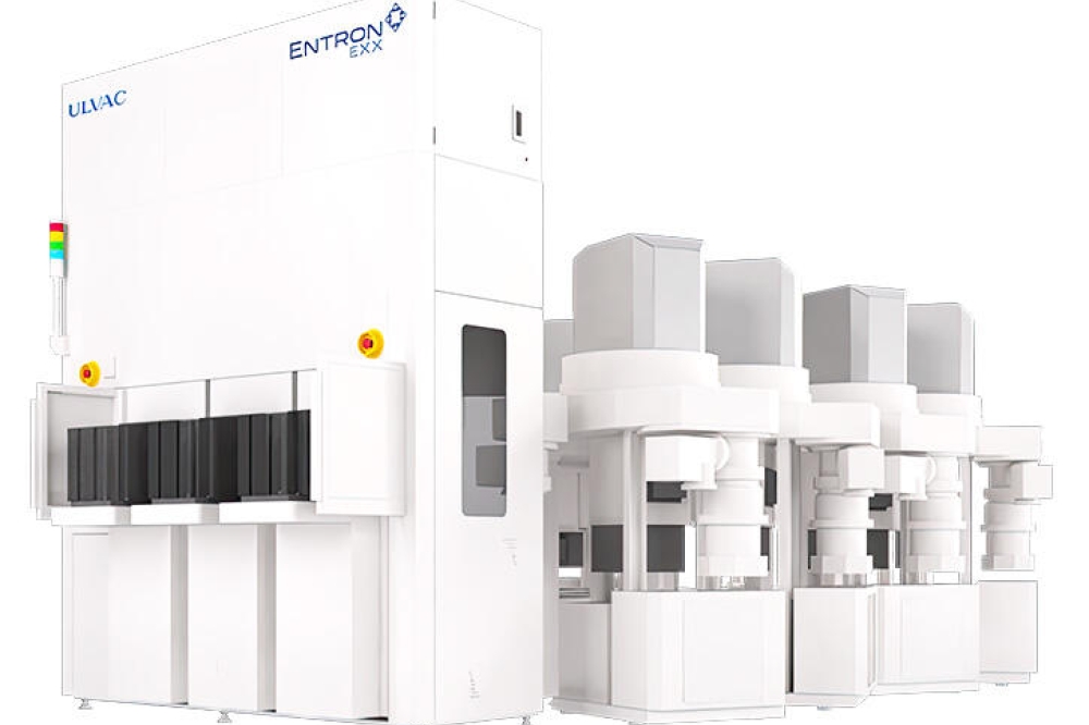
Intel is celebrating the arrival of its Intel 4 technology, which uses extreme ultraviolet (EUV) technology, and the first use of EUV in high-volume manufacturing (HVM) in Europe. The arrival of this important moment ushers in the future for products like Intel’s upcoming Intel® Core™ Ultra processors (code-named Meteor Lake), which will pave the way for AI PCs, as well as future-generation Intel® Xeon® processors coming in 2024 and produced on the Intel 3 process node.
EUV technology employed in the production of Intel 4 is broadly adopted in leading-edge semiconductor technology nodes that power the most demanding computing applications, such as artificial intelligence (AI), advanced mobile networks, autonomous driving, and new data center and cloud applications. EUV plays a critical role in driving Intel toward its goals of delivering five nodes in four years and regaining leadership in process technology by 2025.
“I am proud of the Intel team as well as our customers, suppliers and partners who worked with us to bring this moment to life and keep us on the path back to process leadership,” said Pat Gelsinger, Intel CEO. “The Silicon Isle has always been core to our long-term strategy, and today’s opening of Fab 34 contributes to the EU's goal of creating a more resilient and sustainable semiconductor supply chain.”
A More Sustainable, Resilient and Secure Global Supply Chain
The opening of Fab 34 in Leixlip, Ireland, combined with Intel’s planned wafer fabrication facility in Magdeburg, Germany, and planned assembly and test facility in Wrocław, Poland, will help create a first-of-its-kind end-to-end leading-edge semiconductor manufacturing value chain in Europe. As the home for industries at the vanguard of technology – AI, telecommunications, data center, automotive and others – Europe needs a resilient leading-edge semiconductor supply chain. Intel is committed to helping Europe realize its technological ambitions and, in turn, to building a global semiconductor supply chain that is resilient and geographically balanced.
“Intel’s Ireland operations are a cornerstone of our global manufacturing footprint, and an important part of building an end-to-end semiconductor manufacturing value chain in Europe,” said Keyvan Esfarjani, executive vice president and chief global operations officer at Intel. “As we continue to advance our 17-billion-euro investment, this marks a significant milestone and a win for our Ireland operations as it brings Intel’s latest and greatest Intel 4 technology utilizing EUV to Fab 34, Ireland and Europe.”
Dr. Ann Kelleher, executive vice president and general manager of Technology Development at Intel, said, “This is a landmark for Intel and the semiconductor industry as a whole. The transfer of Intel 4 process technology into high-volume production in Ireland is a giant step toward enabling leading-edge manufacturing in Europe and a huge moment for our technology development teams in Oregon, too.”
The process development and early HVM on Intel 4 technology – which delivers significant improvements in performance, power efficiency and transistor density compared with earlier technologies – was performed in Intel’s development fab in Oregon.
“The opening of Fab 34 marks yet another historic day for Intel and for the team in Ireland. Since arriving here in 1989, Intel has been an anchor of our country’s industrial development, and today the company is once again demonstrating its commitment to delivering leading-edge technology from Ireland,” said Leo Varadkar, Irish Taoiseach. “This milestone comes at a pivotal time for the industry, as Europe puts in place the building blocks to increase its semiconductor capacity. We look forward to the role that Ireland can play in realising the region’s ambitions.”
Intel’s Ambitious Environmental Commitment: A Sustainable Path Forward
Intel is committed to expanding its operations while minimizing its environmental footprint. Today, the company released its Ireland Climate Action Plan, which details efforts to reduce greenhouse gas (GHG) emissions, energy use, water use and waste to landfill.
Leixlip’s Fab 34 is on track to achieve LEED® Gold certification. The new facility incorporates several design innovations for increased sustainability. For example, the buildings will be using a 9-to-1 ratio of heat generated by heat recovery to heat generated by traditional methods, and the majority of cement used during construction was characterized as low carbon due to the integration of recycled content.
The Leixlip campus continues to implement the electricity purchasing strategy for 100% renewable supply, returns 88% of its water to the River Liffey and, in 2022, sent 0.6% of its total waste to landfill. These efforts support Intel’s corporate goals to achieve 100% renewable electricity use across its global operations, net positive water and zero waste to landfills by 2030; net-zero GHG emissions across global operations by 2040; and net-zero upstream GHG emissions by 2050.
Continuing a Proud Tradition of Community Partnership
For more than 30 years, Intel has considered the North Kildare town of Leixlip its home in Ireland. The continued development of the Leixlip campus is only possible through the ongoing support and close collaboration of the local community. In conjunction with the official opening of Fab 34, Intel announced today that it will be donate 1 million euros to the Leixlip community to fund a community project.


