

For die in a package it’s always about the bond
Semiconductor production is so complex that manufacturers constantly seek to reduce costs and improve performance. As advanced node devices continually shrink, process complexity, cost and risk also multiply. Silicon Semiconductor spoke with the experts at Palomar Technologies to learn how die bonding continues to evolve and play a central role in II-VI, III-V, photonic and hybrid module manufacturing.
THE UNIVERSALITY of some semiconductor processes points to their essential nature across technological platforms. Even as device form factors, lithographic innovations, defect management and performance enhancement techniques come and go, there remain some steps that are always needed including the requirement to place finished die inside a receptacle that will protect it and enable its functionality.
As nodes advance to smaller feature dimensions, manufacturers are keenly aware of the growing importance of finely tuning process steps and material formulations to aid in defect elimination and quality control while improving product lifetimes / adding value. This attention to details pays dividends that include enhanced profit margins, faster time to market and reduced cost, not to mention overall customer satisfaction.
Die bonding is a prime example of how a technology that has been a part of semiconductor production predating the advent of widespread automation has continued to evolve and bring value to complex manufacturing systems. In a recent conversation with Palomar Technologies’ Kyle Schaefer, product marketing manager, Silicon Semiconductor technical editor Mark Andrews spoke about ways that die bonding has evolved, and how advances in the field can contribute to balancing the need for high throughput along with process control. This versatility benefits very diverse products that can range from filters to power amplifiers to photonic assemblies.
Schaefer noted that one measure of how die bonding continues to evolve can be found in the RF power amplifier market, which is expected to increase substantially in the next five years. This expectation is rooted in the need to support 5G service rollouts that depend heavily on new power amplifier assemblies in base stations. The estimated CAGR for the general RF power amplifier market is 5-6 percent from 2020-2025. This anticipated demand translates into a need for manufacturers to increase their production capacity. But unlike previous generations, 5G technology is different than the more evolutionary transitions seen as 2G became 3G, which begat 4G; a simple production ramp will not address all 5G needs since volumetric growth carries with it new challenges as well as new processes that need to be developed and refined.

5G vendors must simultaneously churn out considerably more devices while dealing with design, material, and process faults. There is also a great deal at stake in terms of long-term supply chain relationships—5G technology is the foundation of new, wide-ranging commercial initiatives including the opportunity to use wireless networks to fill gaps in wireline networks or supplant fixed broadband access. In the mix are new amplifier designs at higher frequencies and new technologies along with all the usual pressures to ramp-up volumes. A misstep during the early stages of a build-out expected to take a decade or more could freeze-out a manufacturer from future business. Poor execution in terms of yield, quality, or product reliability could indeed prove quite costly if future business tenders fail to convert into design wins.
RF power amplifiers are worth examining in the context of die bonding due to the mixed technologies being utilized. While not as different as requirements for photonic assemblies, there are substantial differences between amplifier types, principally divided between die utilizing LDMOS technology and components based upon newer technologies such as gallium nitride (GaN) on silicon carbide (SiC). While LDMOS is considered mature, GaN on SiC has been a mainstream product for a fraction of the LDMOS tenure. GaN-based amplifiers also serve a substantially different frequency range (3.5 GHz and above), and due to its significantly greater power density, the most important metric for assessing a successful bond for GaN amplifier die comes down to thermal management.
“Ensuring high thermal conductivity of the bond between the chips and the transistor package is paramount to the longevity and performance of the device. Beyond that, the build requirements vary based on assembly approach and materials used,” Schaefer noted. In addition to the thermal management requirements, GaN devices are also more fragile and come at a higher cost than similarly sized LDMOS devices. Due to their fragility and susceptibility to surface damage, pick-place-bond sequences for GaN die need greater care during handling and bonding.
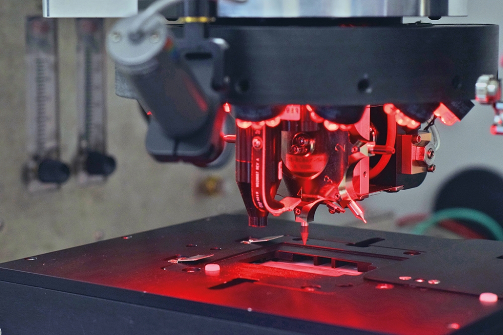
In addition to very significant differences between LDMOS and GaN that affect handling and die attach methodologies, the second most important division concerns the actual assembly and die attach material options. There are a host of choices available, each designed to deliver voidless bonds with high strength and longevity appropriate to the underlying die technology. An important related aspect of die bonding is the vision system used to not only ensure highly accurate and consistent placement, but also help maintain quality while collecting data to ensure damage-free placement of each die. Using Palomar Technologies 3880 Die Bonder as a reference, Schaefer explained ways that industry’s latest bonding systems deliver performance that was previously not possible.
“For preventing component damage in general, or even simply just monitoring die placement, the die bonder vision system can be used to great effect. Often a simple active process control step consisting of a single reference can be enough to prevent repeated misplacement or consecutive component damage. This can be achieved by using a unique feature of the VisionPilot® referencing system referred to as the ability to ‘score clutter’. Essentially, the pattern recognition algorithms can use excess data (i.e. clutter) which comes from debris, chips, and scratches, to lower the given ‘score’ for a reference. This allows rejection of die based on damage or cleanliness.”
“Using this technique before beginning any assembly allows for die sorting during the actual build process to prevent any waste of material. It is also possible to use this same ‘chip damage check’ after placement to avoid any instances where damage was done through any debris collected on the vacuum tool – a situation that, when left unchecked, could result in consecutive device destruction until noticed much later down the line. This control step can also simultaneously check for die placement repeatability in terms of X, Y, and Theta, further adding to the complete control options available,” Schaefer explained.

While some process tools come and go depending on the die generation, others evolve since the need to perform a given function like wafer manipulation remain even as wafer diameters change, die grow smaller, or substrate materials vary in crystalline structure, thickness and fragility. Yet the underlying need to move wafers along a processing line remains even as other factors change. The same could be said with die bonding, hence the favored approach of building a process tool that evolves rather than enters production with only a limited lifetime.
The idea of flexible evolution was central to the development of Palomar Technologies 3880 Die Bonder. Schaefer explained some of the highlights of the system’s enduring and wide-ranging appeal.
“Flexibility is key to providing a strong ROI across many business models from academia, SME’s, CM’s, to full scale manufacturing giants like Lumentum & II-VI. Typically, Palomar customers keep Palomar bonders for many years, so longevity of support and the ease of reconfiguration as products and processes mature and change is a major consideration for engineers and procurement professionals when investing in bonding solutions.”
“Specifically, flexibility is one of the core design philosophies of the Palomar 3880. The flexibility of the system is unique in that it offers the capability to easily change from one process or configuration to another while also remaining effective in its performance for all potential applications.”
“It is not just the 8-position, bi-directional tool turret, which only takes 250ms to change tools on the fly, that makes the 3880 extremely flexible. It is the extra-large work envelop where many configurations of bonding hardware, material presentation options and automation options can be utilized. In addition, the changeover is rapid and effortless which supports any company’s need for high mix.”
“Essentially, the robust abilities of the software and hardware are the core functionality that make the flexibility of the 3880 so impactful, in that it is not just great in one area and good in many others, but it is great in all areas. The 3880 is an R&D, NPI and volume production machine all in one,” Schaefer stated.
As semiconductor processes and manufacturing goals change with succeeding device generations, some needs remain constant, like the requirement to pick and place die, then create a permanent, robust bond between the device and its package. The Palomar 3880 remains a centerpiece of both research and all manner of production environments. Sometimes, the best products just keep getting better.


