

Advanced MES capabilities can extend semiconductor fab lifetimes
As the current global microelectronics shortage demonstrates,
semiconductor manufacturing is not a simple. IC fabs are not created to
pivot quickly as much as they are to produce high quality products at
low cost. The experts from Critical Manufacturing outline ways advanced
manufacturing execution systems (MES) can help fabs maximize output
while also extending their serviceable lifetime.
BY CRITICAL MANUFACTURING
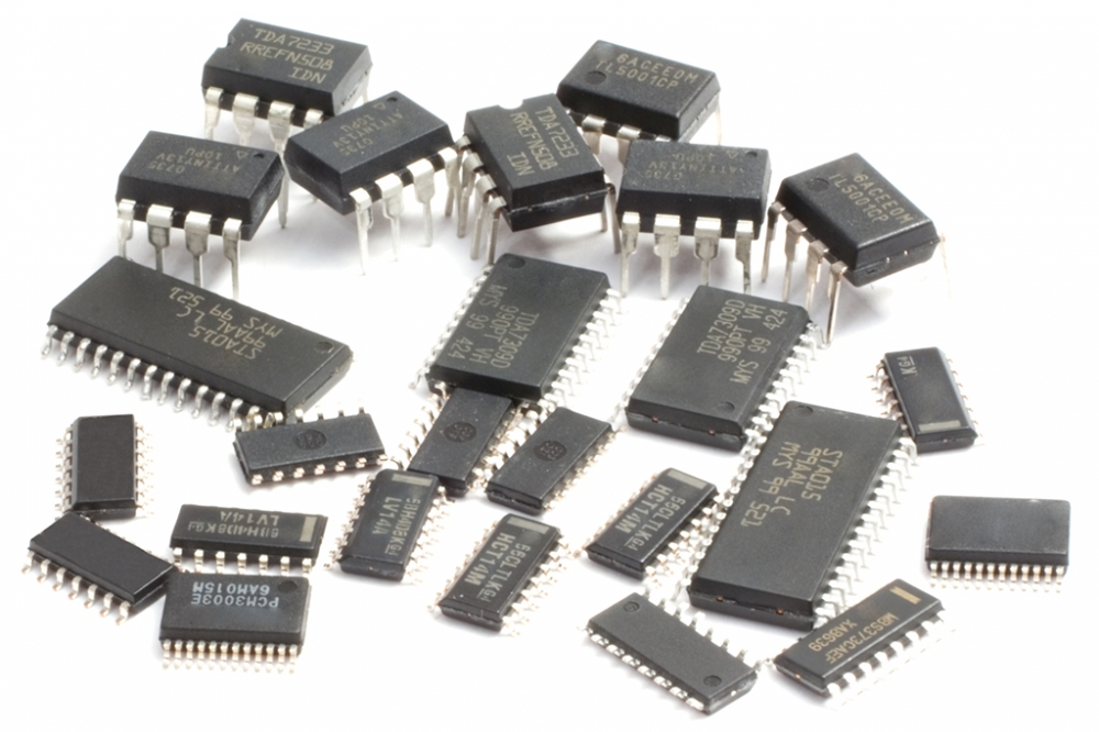
SEMICONDUCTOR MANUFACTURING is unquestionably one of the most complex and sensitive manufacturing processes in the world. Creating line widths on silicon wafers down to five nanometers or less with billions of transistors means that even the smallest vibration or misalignment during fabrication will cause issues. Alongside the sophisticated processes required to manufacture, the industry is further challenged with very short product lifecycles involving millions of devices, or, the need for small batches of niche products to be produced over decades. Only a few semiconductor companies in the world can afford to invest in building new, large capacity fabs with the latest equipment and technologies. Incredibly expensive equipment such as extreme ultraviolet (EUV) scanners costing over $125 million each combined with the need for costly clean room real estate truly makes IC manufacturing one of the most challenging business environments.

One hallmark of a good MES designed to support advanced semiconductor
manufacturing is a simple interface; ideally the interface should be:
intuitive; support multiple production sites; offer multi-lingual
options and provide easy navigation.
For the last two decades, increasing wafer size and performance in front-end chip processing has been an industry focus, with manufacturers looking to more expensive 300mm wafer technology to meet demands for quality, high volume products. But as chips are made and used in an increasing number and variety of products, it has become apparent that not every chip needs to be produced at the millions of unit’s level using the latest technology.
A substantial portion of the ICs made today – even those in advanced products – can still be produced, efficiently and profitably, in smaller 150mm and 200mm fabs, which are experiencing a surprising renaissance in recent years. Many of these smaller fabs started life in the 1990s or even the 1980s; a lot of the equipment dates back to the last century, but still adhere to industry manufacturing standards. This equipment has what some might consider surprising longevity thanks to frequent upgrades, readily available replacement parts and the addition of more sophisticated robots and sensors combined with comprehensive maintenance programmes.
Smart manufacturing is establishing a foothold in the semiconductor industry and Industry 4.0 technologies are breathing new life into aging process tools to make them run even more cost efficiently. By employing modern manufacturing execution systems (MES), the life of aging semiconductor production facilities can be extended, and advanced capabilities can be added to provide a pathway to the future for the industry.
A future-ready MES provides manufacturers with solutions to many challenges. It can add production capacity and throughput by driving efficiency without increasing expensive clean room space. It can enhance production consistency and reduce costly processing errors, reduce time-to-market for new products, and provide solutions to enable the latest, most advanced production steps. Some or all of these benefits may not only be critical for profitability, but may actually be the key to the survival of a company.

In documenting the flow of information and automating such tasks as step change approvals, a simple graphic depiction of hierarchy and process flow (seen here) aids quick comprehension of the task at hand.
Why and which MES
The cost and changing landscape of semiconductor manufacturing needs an MES solution that can adapt for the future. Data is more important than ever and offers manufacturers a way to better monitor and control processes as well as providing deeper insights to help resolve production challenges and support decision making.
As volumes of data continue to increase at a tremendous rate, first and foremost, a future-ready MES needs to incorporate a fully scalable Industrial Internet of Things (IIoT) data platform for ingesting, processing and analyzing the vast volumes of data points that, if contextualized and analyzed correctly, can increase the speed of learning to help drive production efficiency and deliver continuous process improvements.
New fabs and equipment have the capability to be highly automated, but the cost is very high. For older fabs, a modern MES solution presents a way to extend the life of facilities and tools without spending billions of dollars needed to build and equip a new fab. But success requires a highly versatile system that can integrate new IoT devices and legacy equipment to provide full visibility of plant operations. By providing greater control and tighter processing tolerances, the right MES solution can increase production capacity, efficiency and throughput, presenting significant advantages to producers, especially with the current shortage of chips available in the market.

Typical layout of controls with clear access points; MES tools
should always be developed with constant feedback from current and new
users.
Older facilities usually have a legacy MES combined with a patchwork of disparate systems that operators have used over the course of years. Long-term operation within a given environment may build confidence, but it is a fact the maintenance of such older systems that consume a great deal of specialized resources since technology upgrades and additional applications have been added over the years.
Because so many resources are focused on keeping an outdated yet familiar system up and running, it is easy to forget that advanced MES now available could substantially improve an organization’s capability and profitability. This is especially true for situations where businesses have merged or been acquired; fabs in different locations will often have different MES solutions. This adds an additional maintenance layer to the plant’s overhead and inhibits the ability to fully optimize production across multiple sites.
What should older fabs look for from a new MES? One major manufacturer found that bringing disparate systems and processes into a holistic MES solution integrated with ERP delivered substantial benefits. First, it forced them to organize the information and enforce protocols which, in turn, created better understanding and continuous improvement to meet tightening requirements. Having previously used legacy MES technology to guide shop floor processes, the new MES provided much-needed increases in granularity to drive efficiencies. First pass yield increased and cycle times decreased; there was also a beneficial information flow increase, greater visibility into processes and error reduction. Overall, the impact on the bottom line was significant. But perhaps more importantly for the future, the investment made today in a fully scalable MES offers this customer even more ways to reduce costs and increase production capacity through legacy equipment integration and even tighter parameter control while enabling future expansion. Essentially, the customer gained a much more productive present day production environment as well as easier pathways for future expansion.
The ability to compare various aspects of a process recipe with
those under development is a key benefit any good MES should provide its
users.
MES for advanced production scenarios
Master data management
Each product in a fab can require the tracking of thousands of pieces of information about process flow, recipes, parameters, reticles, specifications and sampling, to name a few. A modern MES must have the ability to readily maintain and control these huge volumes of data and provide a complete material history for the final product with full change management and versioning control. It must offer the flexibility to handle common sub-flows with the changes that are made for each layer and provide mechanisms to re-use complete flow blocks while defining appropriate context.
Automatic validation prior to processing
There may be hundreds or even 1,000+ process steps to produce a given semiconductor product, throughout which everything needs to be tracked and checks carried out to ensure there is no misprocessing. Automatic validation prior to processing reduces the risk of errors by validating whether the right product is on the right tool, with the correct recipe and right durable, and the operator has the correct training and authorization.
Multi-chamber tools
Cluster tools have multiple chambers which can run processes in parallel or sequentially, offering significant efficiencies. Tool vendors typically offer different running modes for maximum efficiency, chamber dedication or some engineering use cases. However, these tools require proper modeling and special control logic in the MES to fully take advantage of the complex capabilities. As an example, if any of the chambers are not working, the MES needs to ascertain whether the machine can still be used for any given product. It also needs to be reflected in KPI calculations such as availability, utilization and OEE.
Experiment management
As many semiconductor products have a short lifecycle, engineering modifications and development products can sometimes account for more than 50% of the wafers in production. This requires efficient management of small batches with the ability to adjust process variables and quickly compare results. A Design of Experiments (DoE) module will support processing of experimental wafer groups and allow for the many process variations involved. Integrating this into the MES makes it easy to create experimental runs and execute them together with all other production lots. The inherent tracking and traceability within the MES will further ensure the collection of all necessary data for efficient results evaluation.
Recipe management within the MES universe needs to correspond with key
reference points as set by production managers and any others the
company desires to have access and management privileges.
Recipe management
Front-end semiconductor processing can involve highly complex recipes; ensuring the right recipe is used for a particular product is crucial. An MES with an integrated recipe management system provides users with the ability to centrally manage recipes and their parameters. Additionally, through equipment integration, upload and download recipes to or from equipment as required can be managed more effectively. Automated recipe management prevents human errors and reduces the need for reworking or scraping wafers.
Run-to-run
Feedforward and feedback process control is an essential aspect to increasing yield and enhancing quality. An MES can analyze data from the previous batch to determine if any adjustment to recipe parameters is required to consistently maintain tight tolerances. For example, if the results of an etching process are beginning to drift, it may mean that wafers need to remain in the chemical bath for longer, or that the current needs to be increased to achieve the required process results. For complex run-to-run calculations, the MES should be capable of interacting with a dedicated application, such as Matlab.
Reticle management
Alongside tracking wafers, the MES needs to track reticles and probe-cards, ensuring that the correct durable is used while enabling efficient location of any one of the thousands of durables on the shop floor. It must enforce the use of the correct mask at the appropriate processing step and track usage for maintenance purposes. It needs to include data about the mask within the lot history and provide capability to allocate available or even dedicated masks to different process jobs in line with production scheduling.
Send ahead wafer: Splitting and merging
Sometimes it is required to split a wafer from a cassette to send ahead to test a process. This split, in which a single wafer is processed separately, needs to be tracked but the system also needs to be able to merge the wafer back into the lot afterwards. In some cases, this will not involve a physical split of the wafers. Instead, the whole cassette is moved through the send-ahead path with the MES controlling which slots the equipment needs to process while masking the rest of the wafers. An MES needs to support the creation of a send-ahead run and support the appropriate scenario for the rest of the lot until the success of the process step has been confirmed.
Binning
Although the manner in which wafers that will build microprocessors are manufactured in the same way from one wafer to the next, at the end of processing some chips may perform differently. The most efficient chips can be sold at a higher price. Therefore, it is desirable to grade the chips, which requires the identification of higher and lower performing product. Whether a separate application or part of the MES, binning is a critical production capability.
Container tracking
Whether a cassette, box or FOUP, containers also need to be tracked along with information about their contents. The MES needs to ensure containers are maintained correctly and there is no risk of cross-contamination between processes. It must support the definition of a compatibility matrix between the different contamination classes and automatically increase contamination levels for carriers as they are used. Management of empty containers is important to ensure their timely availability at logistic steps such as lot start, split or transfer.

Monitoring process steps and subcomponent modules should be direct with
clear access commonalities whether being utilized on the production
floor or in management centers.
Time constraints
Many front-end manufacturing processes are time sensitive. Also, the time between certain steps very often needs to be monitored as well so that no one step significantly departs from its established tolerance range. The MES must support the definition of process queue time constraints between any process step and ensure all time constraints are adhered to and when they are not, a warning needs to be issued and error rules should come into play if time parameters are violated.
Tool dedication
Busy semiconductor production fabs often need to prioritize certain lots or allocate machines based on their performance on certain product types. A modern MES must support a generic mechanism to set in advance which equipment (chamber, durable, etc.) must be used to process a lot at a particular process step.
Summary
The complexity and variability of front-end semiconductor processing requires a feature-rich but highly flexible MES. A solution should be adaptable to all production scenarios and provide ready scalability to the increasing volumes of data coming from equipment and sensors. With the current high market demand for semiconductors, a modern MES can help older fabs maintain profitable service while extending the life of their tools and operations. It can increase the capabilities of smaller wafer fabs, increase yields, reduce processing errors and increase production speeds. It offers a way to efficiently manage the available data, derive value from it and provide the flexibility to handle adding new sensors, equipment and application modules in the future. An advanced MES is purpose-built for configurability, flexibility and straightforward deployment. Once properly deployed, the MES can reduce overhead costs of managing production systems while extending life of older fabs.


