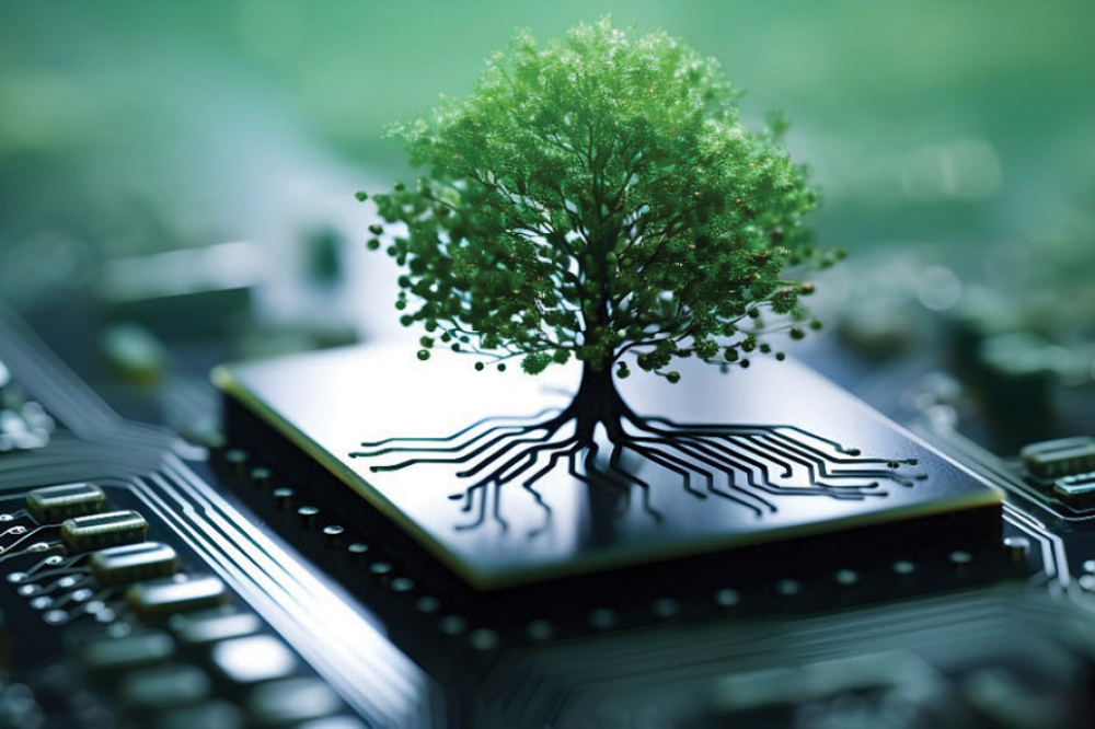
Semiconductor solutions from Pfeiffer Vacuum
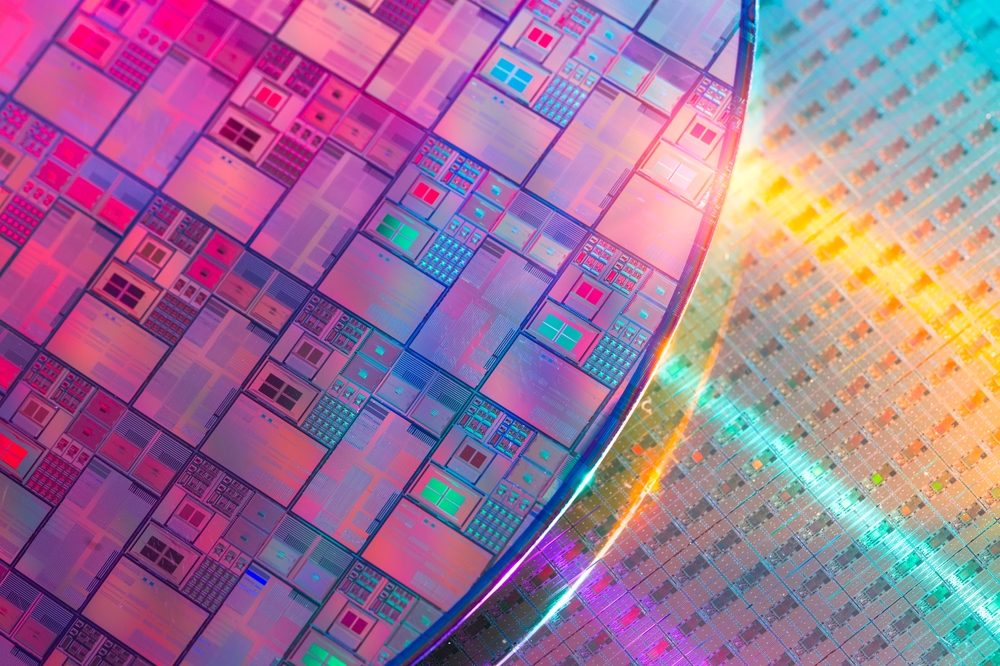
Semiconductor fabrication takes place under clean-room conditions in the high and ultra-high vacuum range. To ensure that these conditions are met, reliable vacuum equipment is a must.
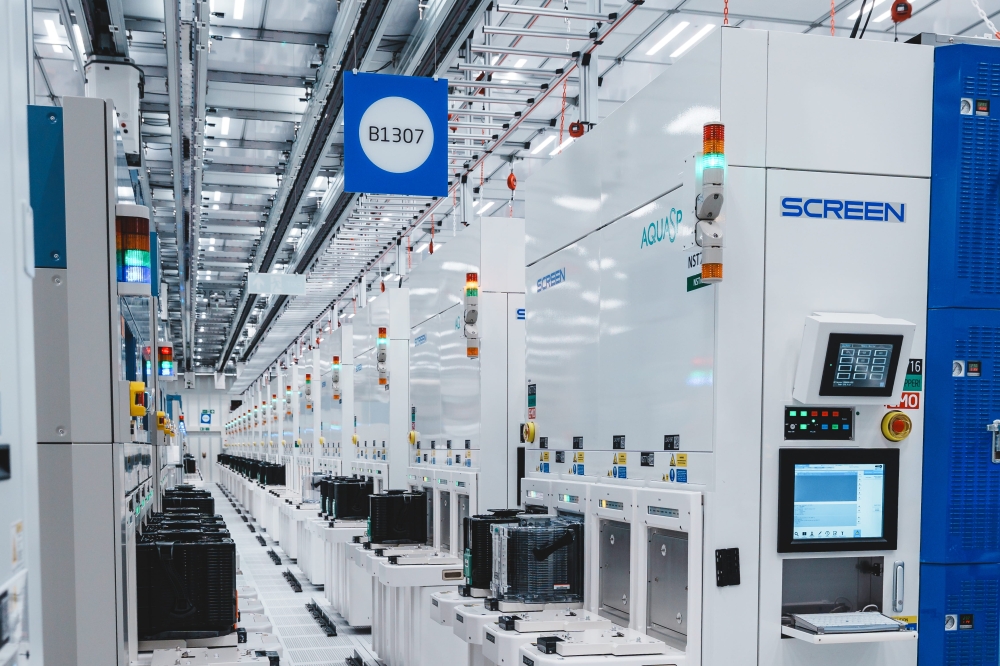
A typical semiconductor fab consists of four levels. At the top level, the cleanroom, the production line as well as special systems for contamination management are located. The level below the cleanroom – the so-called “subfloor” – is where the dry pumps for the evacuation of load-locks and transfer chambers are located. The next level below is where the cooling units, current supplies and RF-generators of the plant are located. The lowest level contains dry pumps and the exhaust gas treatment (abatement) equipment.
Explore our solutions for semiconductor fabs – in 3D and from a 360° perspective! Click through the different floors and components of our semiconductor fab model and learn which products Pfeiffer Vacuum offers to fulfill the diverse requirements! https://www.pfeiffer-vacuum.com/en/solutions/vacuum-experience/semiconductor-fab-3d/
Deposition
Manufacturing of a semiconductor component is a very complex process, involving many steps under vacuum. The deposition process is one of them and consists of depositing a material on the wafer through several technologies: PVD (Physical Vapor Deposition), PECVD (Plasma Enhanced Chemical Vapor Deposition), SACVD (Sub-Atmospheric Chemical Vapor Deposition), LPCVD (Low Pressure Chemical Vapor Deposition) or more recently ALD (Atomic Layer Deposition). Each technology requires a different level of vacuum. We provide high vacuum turbopumps and primary dry pumps solutions dedicated to your deposition applications and designed for the lowest cost of ownership and highest process lifetime.
Applications
- PVD (Physical Vapor Deposition)
- PECVD, SACVD
- Diffusion, LPCVD
- ALD (Atomic Layer Deposition)
Etch & Clean
Manufacturing of a semiconductor component is a very complex process, involving many steps under vacuum. Dry etch process is one of them and consists of selectively removing a material on the wafer. This material can either be a conductor material, shaping the structure of the semiconductor component, or a dielectric material, insulating the conducting parts of the component. Strip & Clean processes are also used to remove selective materials from wafer surface, such as photoresist film and residues that could impact the device performance. Each technology requires a different level of vacuum. We provide high vacuum turbopumps and primary dry pumps solutions dedicated to Etch & Clean applications and designed for the lowest cost of ownership and highest process lifetime.
Applications
Dry Stripping & Cleaning
Dielectric Etch
Conductor & Polysilicon Etch
ALE
Ion implantation
Manufacturing of a semiconductor component is a very complex process involving many steps under vacuum. Among them, ion implantation process consists of doping the silicon wafer surface with ions, to change the electrical characteristics of the material and increase device conductivity. Regardless of implanter technologies (medium current, high current or high energy), implanter tools layout includes three main vacuum areas: Ion source, beamline and end station. We provide high vacuum turbopumps and primary dry pumps solutions for all implant applications and are designed for the lowest cost of ownership and highest process lifetime.
Applications
Source, beamline & end-station
Wafer handling
Manufacturing of a semiconductor component is a very complex process, involving many steps under vacuum environment. Wafers enter or exit a semiconductor tool through load-lock chambers to ensure the right vacuum level. Wafers are moved from process chamber A to B through transfer modules, which are also maintained under vacuum. We provide high vacuum turbopumps and primary dry pumps solutions dedicated to wafer handling applications and designed for the highest throughput and lowest operating costs.
Applications
Load lock & transfer
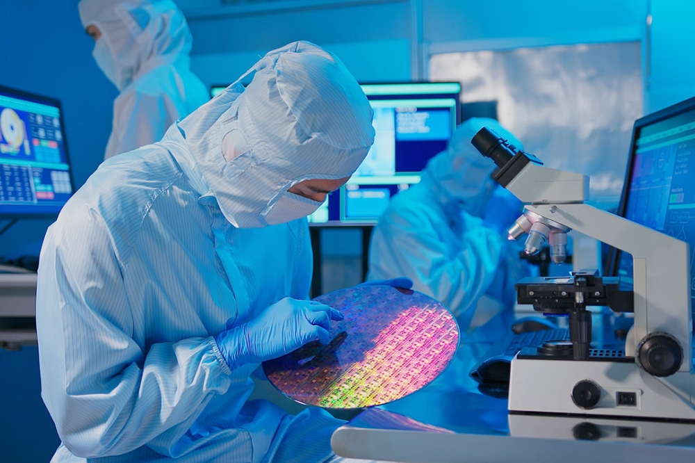
Inspection & Metrology
As semiconductor device manufacturing become more and more complex with increased number of steps, wafer inspection and metrology are more critical than ever. Besides vacuum solutions for traditional inspection & metrology tools, we provide innovative in-line Airborne Molecular Contamination (AMC) systems for Front Opening Universal Pods (FOUP) and clean room environment analysis. With our AMC systems, wafers are analyzed through the production cycle, contributing to increase manufacturing yield.
Applications
CD SEM
AMC and particles monitoring in FOUP
AMC monitoring in clean room
Lithography
Manufacturing of a semiconductor component is a very complex process. Photolithography process is one of them and consists of defining and transferring patterns in each layer of the device. As chip node dimensions continuously shrink, traditional photolithography using Ultra Violet (UV) light has reached its limits. A new lithography process using Extreme Ultra Violet light (EUV) under vacuum has emerged. We provide high vacuum turbopumps and primary dry pumps solutions dedicated to EUV application, supporting advanced chip scaling below 10 nm node.
Applications
EUV (Extreme Ultra Violet) lithography
Facilities & Maintenance
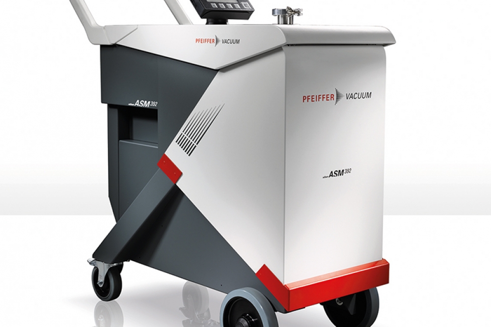
Any single leak present on a semiconductor tool and its related facilities can impact manufacturing throughput and yield. Consequences vary from loss of production due to process specs not met, to critical safety hazard. Therefore, leak detection is a critical and mandatory step of any new tool commissioning in the clean room or after any maintenance intervention. At the basement level, forelines & dry pumps are also regularly exchanged for cleaning or repair. We provide comprehensive leak detection solutions which guarantee vacuum integrity of your installation from process chambers down to gas abatement. Our goal: Maximize your production yield.
Applications
Leak Detection
Pfeiffer Vacuum
Nashua, NH
Tel: 800-248-8254
www.pfeiffer-vacuum.com
E-mail: contact@pfeiffer-vacuum.com