
amcoss wafer processing tool contributes to increase in productivity
amcoss GmbH, based in Feldkirch, Austria, has supplied Jenoptik in Berlin-Adlershof with a fully automatic amc 2000 wafer processing unit for coating and developing of wafers. Being one of the leading manufacturers for high-power, edge-emitting semiconductor lasers, Jenoptik will use the equipment in lithography processes.
“The amcoss equipment is a replacement tool. Our goal is to significantly increase capacity and yield, compared to the tool we have been using so far, which will noticeably raise productivity. Furthermore, we need optimized wafer centering and more flexible application possibilities for 3” and 4” wafers. With amc 2000 we are sure to reach these goals and to even increase quality and efficiency in wafer processing”, says Dr. Jürgen Sebastian, site manager of Jenoptik Berlin where high-power diode lasers for medical applications, materials processing, R & D and as pump sources for solid-state lasers are being produced.
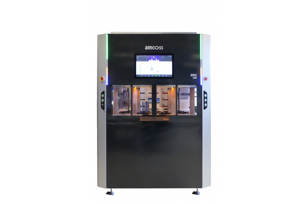
amcoss wafer processing equipment is configured according to individual customer needs and demands. Every tool is unique. “We do not build mass products, but each of our machines is a highly complex single piece. That is our strength,” explains company owner David Erne. “So, amc 2000 for Jenoptik has been designed for highest throughput. With its dual arm handler and 4 loadport stations for parallel operation of up to four processes, it absolutely is a high-throughput tool.” Besides a space-saving, integrated alignment-on-the-fly, a prealigner may be alternatively used, if flat- orientation were necessary.
Utmost flexibility regarding wafer diameters and applications
Another reason to decide for an amcoss amc 2000 equipment is its absolutely flexible layout. It is a veritable bridge tool. Jenoptik is now capable to simultaneousely process different wafer sizes – especially the necessary 3” and 4” diameters – without adaptations when changing to another size. By fitting the tool with 5 dispense lines with an innovative, unique single-nozzle-gripper system and an additional syringe, flexibility has increased even more. Various Hot- and Coolplates, a special Vapor Prime Hotplate and an efficient EBR system, top off the configuration.
“We are very pleased, that a renowned company like Jenoptik has chosen us as their partner”, says David Erne. “The quality of their industry-leading diode lasers is based on most advanced manufacturing methods and process technologies, which we are delighted to support with our equipment and processes.”
In addition to the new amcoss wafer processing tool, an amc 2500 equipment by amcoss has been installed at the Jenoptik site in Dresden. So, sustainable support for equipment in use, as well as synergies for longterm service are guaranteed.
amcoss GmbH develops and manufactures completely customized fully- or semi-automatic processing equipment for coating, developing, temperature control and cleaning, as well as lift-off and etching of substrates and masks from a great variety of materials.
Jenoptik with its division Light & Optics is a globally operating OEM supplier of system solutions and products based on photonics technologies. The company disposes of vast expert knowledge in optics, laser technology, digital image processing, opto-electronics and software. Under its brand name TRIOPTICS, Jenoptik offers optical measuring- and production systems for quality control of lenses, objective lenses and camera modules.


