ClassOne Technology Announces New Surface Preparation Technologies
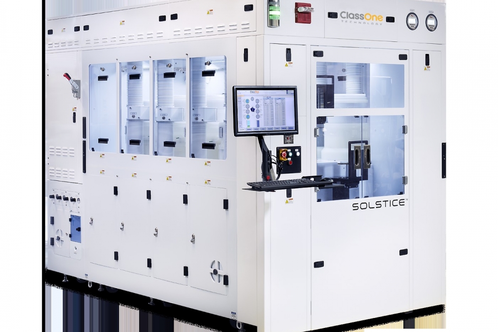
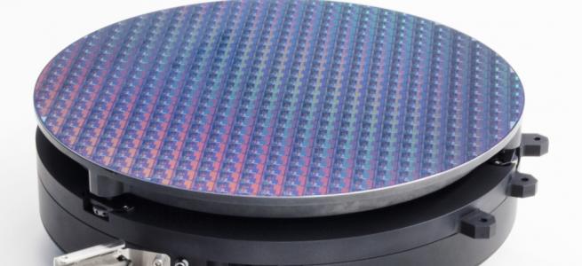
ClassOne Technology, a global provider of advanced electroplating and wet processing tools for microelectronics manufacturing, has announced it has expanded its flagship Solstice automated single-wafer platform with a suite of surface preparation (SP) technologies. On the same proven platform, the company now delivers key SP technologies – including solvent strip, wet etch, metal liftoff (MLO) and single-wafer cleaning – for compound semiconductors and other critical applications requiring ultimate wafer uniformity and process control in a single flexible and compact system.
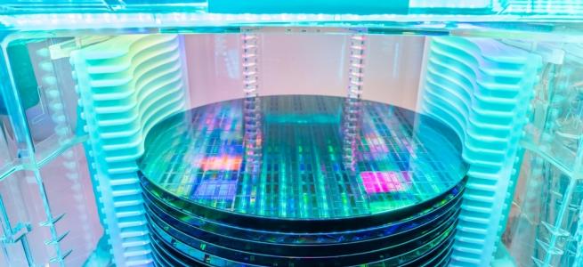
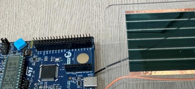
Automated single-wafer processing is growing in value for both within-wafer and wafer-to-wafer uniformity of microelectronic devices, from silicon ICs to compound semiconductors such as silicon carbide (SiC) and gallium nitride (GaN). These advanced devices are increasingly being deployed in such fast-growing markets as automotive, internet of things (IoT), power, and 5G communications. ClassOne is positioned to capitalize on this trend with the expansion of its Solstice platform, broadening customer access to its advanced wafer-processing capabilities.
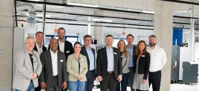
“We are an early adopter of the Solstice platform, and ClassOne has been always a reliable, responsive, and supportive partner,” said Matthias Lessel, head of deposition and cleaning at TRUMPF Photonic Components. “Over the years, the Solstice platform has proven its advanced performance capability for surface preparation. In particular, the face-down architecture is optimized for safety and performance, while the platform’s class-leading footprint is ideally suited to accommodate our fab constraints. Solstice will remain one of our key contributors to developing our next-generation VCSELs and other photonic components.”
Elegantly designed from the ground up to deliver an unparalleled price/performance ratio, Solstice continues to fill a specific market need as one of the most flexible wet-processing platforms available. Customers can choose a modular configuration with up to 8 chambers for multiple plating, solvent and wet etch applications on the same frame. For volume manufacturing, purpose-built configurations provide optimized design for maximum throughput and cost of ownership. This approach allows ClassOne to serve customers at both R&D low-volume operations and high-volume manufacturing. It also makes ClassOne the ideal partner for customers currently in R&D who are preparing to move to volume manufacturing in the future.
ClassOne has sold or installed more than 400 Solstice reactors since the product’s inception. Moreover, the company’s business has grown 40 percent year-over-year, due in large part to the company’s recent development efforts focused on advancing the Solstice single-wafer platform as its core technology offering.
“At ClassOne we are hyper-focused on technology innovation. As an established leader in electroplating, we are now applying our expertise to surface preparation,” stated Byron Exarcos, CEO, ClassOne Technology. “Expanding our Solstice platform is part of our long-term technology roadmap to address emerging market needs and offer our customers increased capability, flexibility and ROI. We know customers need flexibility in the fab more than ever, regardless of where they are in their production cycles, so offering a scalable solution that can help them grow and deliver top-quality devices is our highest priority.”
Solstice SP Benefits
Solstice SP features a face-down wafer processing scheme. This architecture allows for direct chemistry impingement on the wafer surface, enabling high speed and uniformity of etch, strip, and MLO processes. It also gives Solstice SP a huge safety advantage compared to common face-up architectures, as the fully sealed chambers efficiently drain and exhaust dangerous chemistry. The platform also easily integrates technology for temperature and concentration bath control, allowing for consistent wafer processing and extended bath life.
Additionally, the optional white light End Point Detection (EPD) feature provides efficient processing for film-removal etch, e.g., under-bump metallization (UBM) etch or seed etch. The FaceUp spin rinse dry (SRD) module mounts above the process chambers and provides fast, clean dries because of its chemically segregated location at the top of the tool. When it comes to safety, performance, and reliability, Solstice SP brings a wide array of capabilities for ClassOne’s customers.
All Solstice single-wafer platform options are available now. Pricing varies depending on configuration and chemistry requirements.
To schedule a demo, please contact sales@classone.com, or visit ClassOne Technology in booth #1341 at SEMICON West in San Francisco, July 11-14, 2022.