NEDO approves Rapidus’ FY2024 Plan and Budget
Rapidus says that the New Energy and Industrial Technology Development Organization (NEDO) has approved its FY2024 plan and budget.
Rapidus says that the New Energy and Industrial Technology Development Organization (NEDO) has approved its FY2024 plan and budget for “Research and Development of 2nm-generation semiconductor integration technology and short TAT manufacturing technology based on Japan-US collaboration” under ” Post 5G Information and Communication Systems Infrastructure Enhancement R&D Project / Development of Advanced Semiconductor Manufacturing Technology (Commissioned).” In addition, NEDO has selected its proposal for “Development of Chiplet, Package Design, and Manufacturing Technology for 2nm-Generation Semiconductors.
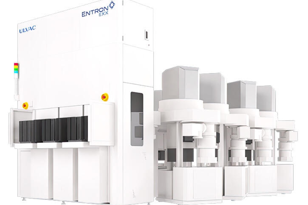
In November 2022, Rapidus’ proposal was selected as a next-generation semiconductor R&D project for the “Research and Development of 2nm-generation semiconductor integration technology and short TAT manufacturing technology based on Japan-US collaboration.” Based on this project, Rapidus started construction of the IIM (Innovative Integration for Manufacturing), a manufacturing base in Chitose City, Hokkaido, and is developing mass production technology for 2nm-generation logic semiconductors by dispatching engineers to IBM Corporation, and achieved the target for FY2023. Furthermore, with the approval of this fiscal year plan and budget, Rapidus will start clean room operation and introduce EUV lithography machines and other manufacturing equipment in preparation for the pilot line operation starting in April 2025.
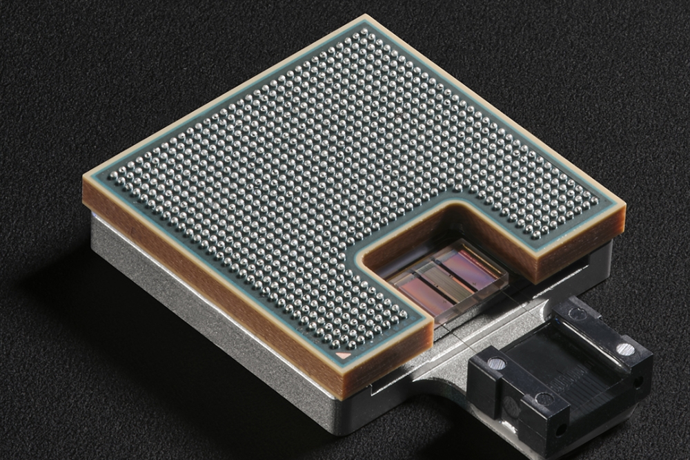
With the selection of this proposal for the “Development of Chiplet and Package Design and Manufacturing Technology for 2nm-Generation Semiconductors,” Rapidus will develop design and manufacturing technology for chiplet packages with the aim of establishing design kits and chiplet test technology, which are necessary for mass production and designs of chiplet packages that achieve larger size and lower energy consumption through the use of 2nm generation semiconductors.
These back-end process areas require innovation in tandem with the development of cutting-edge semiconductors in the front-end process. Rapidus aims to provide its customers with a Rapid and Unified Manufacturing Service (RUMS), which will enable short TAT semiconductor manufacturing by providing design support and integrated front-end and back-end processes.
For the back-end process, Rapidus will utilize a part of Seiko Epson Corporation’s Chitose Plant (758-173 Bibi, Chitose City, Hokkaido), which is adjacent to the IIM under construction in Bibi World, an industrial park in Chitose City, to conduct pilot stage research and development.
Rapidus will establish its business as a domestic foundry featuring short TAT production to secure domestic supply of advanced logic semiconductors, which are the key to economic security, and contribute to enhancing Japan’s industrial competitiveness and boosting convenience in national life.


