
Samsung Electronics to establish Texan semiconductor ecosystem
Proposed CHIPS investment of up to $6.4 billion would complement more than $40 billion in private investment to support a comprehensive semiconductor cluster for logic, advanced packaging, and R&D in Taylor, Texas, and expansion of Austin Fab in Texas.
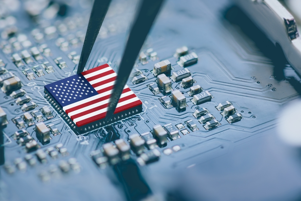
The Biden-Harris Administration has announced that the U.S. Department of Commerce and Samsung Electronics (Samsung) have signed a non-binding preliminary memorandum of terms (PMT) to provide up to $6.4 billion in direct funding under the CHIPS and Science Act to strengthen the resilience of the U.S. semiconductor supply chain, advance U.S. technology leadership, and fuel U.S. global competitiveness. Samsung – the only leading-edge semiconductor company that is a leader in both advanced memory and advanced logic technologies – is expected to invest more than $40 billion dollars in the region in the coming years, and the proposed investment would support the creation of over 20,000 jobs.
The proposed investment would turn Samsung’s existing presence in Texas into a comprehensive ecosystem for the development and production of leading-edge chips in the United States, including two new leading-edge logic fabs, an R&D fab, and an advanced packaging facility in Taylor, as well as an expansion to their existing Austin facility. It also demonstrates Samsung’s ongoing commitment to the United States, where it has been manufacturing chips since 1996. By continuing to develop the technologies of the future in the United States, Samsung is taking steps that would work towards strengthening U.S. economic and national security and increasing the resilience of both the U.S. and global semiconductor supply chains. Because of investments like Samsung’s, the United States is projected to be on track to produce roughly 20% of the world’s leading-edge logic chips by 2030.
“I signed the CHIPS and Science Act to restore U.S. leadership in semiconductor manufacturing and ensure America’s consumers, businesses, and military maintain access to the chips that underpin our modern technology,” said President Biden. “This announcement will unleash over $40 billion in investment from Samsung, and cement central Texas’s role as a state-of-the-art semiconductor ecosystem, creating at least 21,500 jobs and leveraging up to $40 million in CHIPS funding to train and develop the local workforce.”
“Thanks to President Biden’s CHIPS Act, Samsung is expected to invest more than $40 billion to build a cluster of semiconductor factories here in the U.S. that will employ thousands of workers in good-paying jobs, support a robust supplier ecosystem, and fuel innovation through R&D,” said U.S. Secretary of Commerce Gina Raimondo. “Proposed CHIPS investments like the ones we are announcing today will be a catalyst for continued private sector investments to help secure the long-term stability we need to put America at the beginning of our semiconductor supply chain and to safeguard a strong resilient ecosystem here at home. The chips that Samsung will be making in Texas are important components to our most advanced technologies, from artificial intelligence to high-performance computing and 5G communications. With President Biden’s leadership and Samsung’s commitment to the U.S., this proposed funding advances America’s leadership in semiconductor manufacturing on the world stage.”
President Biden signed the bipartisan CHIPS and Science Act to usher in a new era of semiconductor manufacturing in the United States, bringing with it a revitalized domestic supply chain, good-paying jobs, and investments in the industries of the future. The proposed CHIPS investment in Samsung would propel Central Texas into a state-of-the-art leading-edge ecosystem, creating over 17,000 construction jobs and more than 4,500 good-paying manufacturing jobs within the next five years, while stimulating regional commercial growth, leveraging the robust two-year and four-year academic footprint in the state to produce the skilled workers needed to fill the critical roles created by the proposed investment. With these proposed investments and the formation of this ecosystem, CHIPS for America would be helping to deliver on the CHIPS Vision for Success and contributing to the development of the local communities across Central Texas.
“Semiconductor research and development is critical to building a robust and thriving semiconductor manufacturing industry in the United States,” said Under Secretary of Commerce for Standards and Technology and National Institute of Standards and Technology Director Laurie E. Locascio. “Samsung’s plans to build a cutting-edge R&D and advanced packaging facilities in Texas are shining examples of the types of R&D projects that will help build, and heavily contribute to, America’s chip manufacturing industry.”
“We’re not just expanding production facilities; we’re strengthening the local semiconductor ecosystem and positioning the U.S. as a global semiconductor manufacturing destination," said Kye Hyun Kyung, President and CEO of the Device Solutions (DS) Division at Samsung Electronics. "To meet the expected surge in demand from U.S. customers, for future products like AI chips, our fabs will be equipped for cutting-edge process technologies and help advance the security of the U.S. semiconductor supply chain.”
The proposed investment would be split across multiple projects at two separate locations in Central Texas:
• Taylor, Texas: Construct a comprehensive advanced manufacturing ecosystem, ranging from leading-edge logic to advanced packaging to R&D, transforming the small municipality of Taylor into an expansive hub of leading-edge semiconductor manufacturing. This ecosystem would include two leading-edge logic foundry fabs focused on mass production of 4nm and 2nm process technologies, an R&D fab dedicated to development and research on technology generations ahead of nodes currently in production, and an advanced packaging facility producing 3D High Bandwidth Memory and 2.5D packaging, both of which have critical artificial intelligence applications. The semiconductors that are designed and manufactured in this ecosystem would serve a wide variety of end markets – from communications, automotive, and defense industries to high-performance computing and artificial intelligence.
• Austin, Texas: Expand a facility that has been an economic engine for Central Texas for nearly 30 years. This proposed investment would expand the existing facilities to support the production of leading fully depleted silicon-on-insulator (FD-SOI) process technologies for critical U.S. industries, including aerospace, defense, and automotive. This proposed investment also includes commitments to collaborate with the U.S. Department of Defense.
Samsung has a proven record of workforce engagement in Texas, including robust partnerships with local education institutions — such as Austin Community College, The University of Texas at Austin, Texas A&M University, Texas State Technical College, Temple College, Manor High School and Taylor High School — to train its future semiconductor workforce. The proposed CHIPS investment also includes up to $40 million in dedicated workforce funding. Additionally, to attract and maintain the skilled workforce necessary for its projects, Samsung is exploring options in collaboration with the Department to build supply and defray the cost of high-quality and accessible child care for its employees.
Samsung’s waste management efforts at its Austin site have received the Zero Waste to Landfill Gold Level certification for recycling or reusing 96% of waste and its wastewater pretreatment practices have received longstanding recognition from the City of Austin. The Taylor site would use leading-edge sustainability strategies to promote carbon-free electricity use, conserve water resources, and avoid or reduce other impacts to the environment.
In addition to the proposed direct funding of up to $6.4 billion, the company has indicated that it plans to claim the U.S. Department of the Treasury’s Investment Tax Credit, which is expected to cover up to 25% of qualified capital expenditures.
As explained in its first Notice of Funding Opportunity, the Department may offer applicants a PMT on a non-binding basis after satisfactory completion of the merit review of a full application. The PMT outlines key terms for a CHIPS incentives award, including the amount and form of the award. The award amounts are subject to due diligence and negotiation of a long-form term sheet and award documents and are conditional on the achievement of certain milestones. After the PMT is signed, the Department begins a comprehensive due diligence process on the proposed projects and continues negotiating or refining certain terms with the applicant. The terms contained in the long-form term sheet and the final award documents may differ from the terms of the PMT being announced today.


