PI contributes to technology node development
Contributes to EU-funded project 14ACMOS: for semiconductor manufacturing.
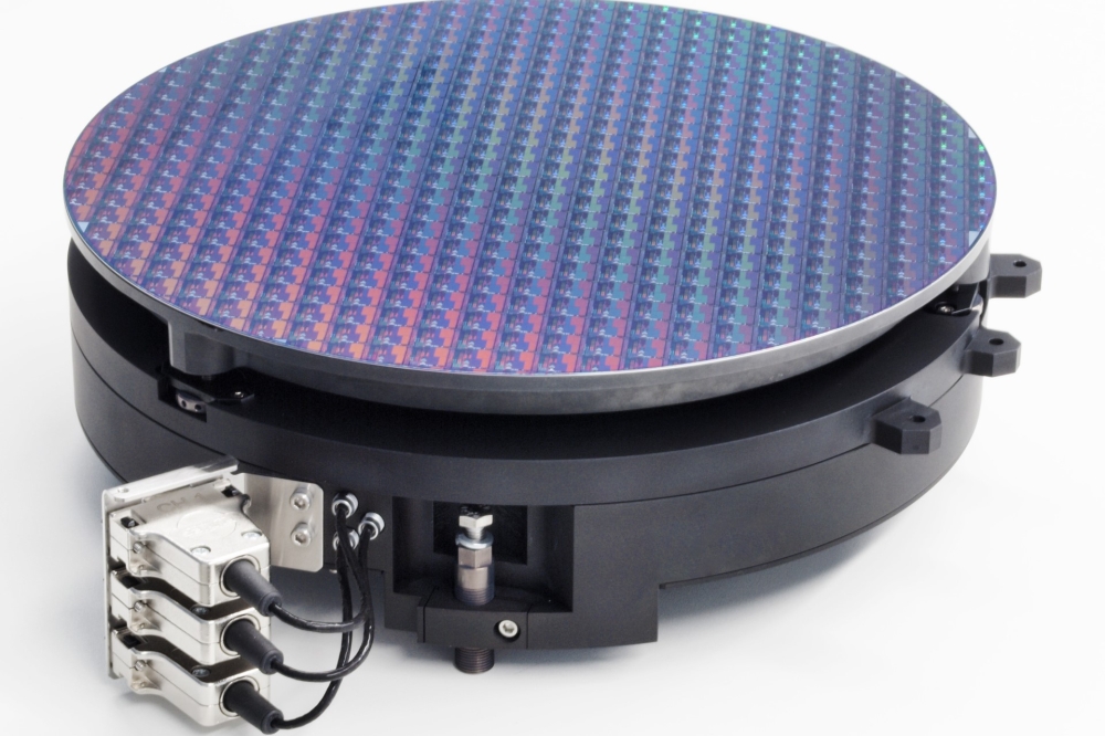
Traditionally, key manufacturing technologies for semiconductor production have come from Europe. To ensure that this does not change in the future, the European Union is funding the 14ACMOS project to develop the next technology node. It is expected that this node will enable the production of chip structures with dimensions down to 14 angstroms. Physik Instrumente (PI) participates in the research program by developing high-precision positioning systems with accuracies of less than one millionth of a millimeter.
High-end microchips manufactured using 3 nm technology are the current state of the art. Production technologies for the 2 nm technology node are expected to be available as early as next year and for 1.4 nm, i.e., 14 angstroms, by 2027. The 95-million-euro research project 14ACMOS is co-funded by the European Union and supported by the “Joint Undertaking for Chips” (Chips JU). It brings together the know-how and development expertise of Europe's leading suppliers to the semiconductor industry. The project, which involves twenty-five partners from six countries, is coordinated by ASML, the Dutch world leader in lithography systems for semiconductor manufacturing.
PI has been a system partner to the semiconductor industry for decades and is represented worldwide with positioning systems in a wide range of areas of semiconductor production. In areas such as lithography and metrology for quality control, the nanopositioning specialist's products are already in use. The positioning systems to be developed as part of the 14ACMOS project must also function precisely and highly dynamically under vacuum conditions in order to be economically viable.


