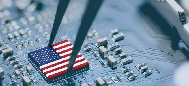
Lam Research, Entegris, Gelest Team Up to Advance EUV Dry Resist Technology

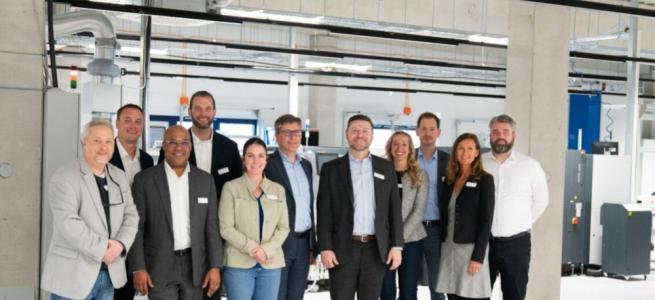
Lam Research, Entegris, and Gelest, Inc, a Mitsubishi Chemical Group company, have announced a strategic collaboration that will provide semiconductor manufacturers worldwide with reliable access to precursor chemicals for Lam’s breakthrough dry photoresist technology for extreme ultraviolet (EUV) lithography, an innovative approach used in the production of next-generation semiconductors. The parties will work together on EUV dry resist technology research and development (R&D) for future device generations of logic and DRAM products that will help enable everything from machine learning and artificial intelligence to mobile devices.
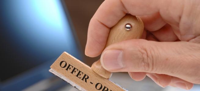
A robust supply chain for process chemicals is critical to EUV dry resist technology integration into high-volume manufacturing. This new long-term collaboration further broadens the growing ecosystem for dry resist technology and will provide dual-source supply from semiconductor material leaders with provisions for continuity of delivery in all global markets.
In addition, Lam, Entegris, and Gelest will work together to accelerate the development of future cost-effective EUV dry resist solutions for high numerical aperture (high-NA) EUV patterning. High-NA EUV is widely seen as the patterning technology that will be required for continued device scaling and advancement of semiconductor technology over the coming decades. Dry resist provides the high etch resistance and tunable thickness scaling of deposition and development necessary to support high-NA EUV’s reduced depth of focus requirements.
“Dry resist technology is a breakthrough that shatters the biggest barriers to scaling to future DRAM nodes and logic with EUV lithography,” said Rick Gottscho, executive vice president and chief technology officer of Lam Research. “This collaboration brings together Lam’s dry resist expertise and cutting-edge solutions with material science capabilities and trusted supply channels from two industry precursor chemical leaders. This important expansion of the dry resist ecosystem paves the way for exciting new levels of innovation and high-volume manufacturing with the technology.”
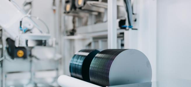
First developed by Lam in collaboration with ASML and IMEC, dry resist extends the resolution, productivity, and yield of EUV lithography, thereby addressing key challenges associated with creation of next-generation DRAM and logic technologies. It provides superior dose-to-size and dose-to-defectivity performance, enabling higher EUV scanner productivity and lower cost of ownership. In addition, Lam’s dry resist process offers key sustainability benefits by consuming less energy and five to ten times less raw materials than traditional resist processes.
“Lam’s dry resist approach reflects key innovations at the material level and offers a wide range of advantages, including better resolution, improved cost-efficiency and compelling sustainability benefits,” said Bertrand Loy, chief executive officer of Entegris. “We are proud to be a part of this innovative collaboration to accelerate dry resist adoption and to be a trusted process materials supplier for customers as they push to create the next generation of semiconductors with this important technology.”
“Our collaboration with Lam and Entegris to advance dry resists for EUV lithography demonstrates our commitment to support chipmakers as they innovate in materials science,” said Jonathan Goff, president of Gelest, a Mitsubishi Chemical Group company. “We’ve seen EUV demonstrate exceptional value in recent years, and we’re pleased to be part of the growing ecosystem to extend its potential.”