STMicroelectronics and GlobalFoundries announce new 300 mm manufacturing facility in France

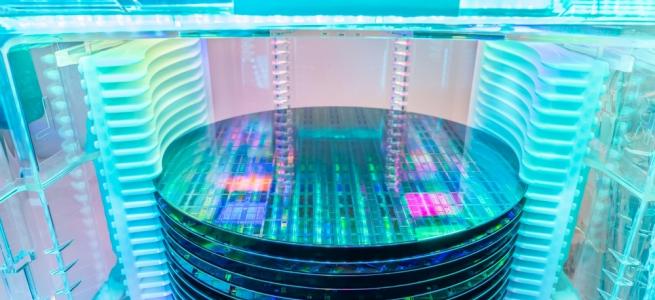
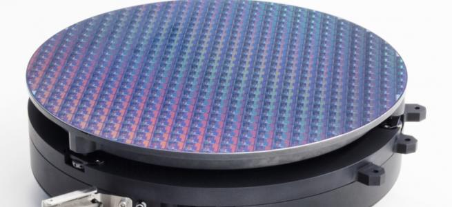
ST and GF are committed to building capacity for their European and global customer base. This new facility will support several technologies, in particular FD-SOI-based technologies, and will cover multiple variants. This includes GF’s market leading FDX technology and ST’s comprehensive technology roadmap down to 18nm, which are expected to remain in high demand for Automotive, IoT, and Mobile applications for the next few decades.
FD-SOI technology has origins in the Grenoble (France) area. It has been part of ST technology and product roadmap in its Crolles facility since the early beginnings, and it was later enabled with differentiation and commercialized for manufacturing at GF’s Dresden facility. FD-SOI offers substantial benefits for designers and customers, including ultra-low power consumption as well as easier integration of additional features such as RF connectivity, mmWave and security.
ST and GF will receive significant financial support from the State of France for the new facility. This facility will strongly contribute to the objectives of the European Chips Act, including the goal of Europe reaching 20% of worldwide semiconductor production by 2030. In addition to the sizeable, multi-year investment in advanced semiconductor manufacturing in Europe, it will support the leadership and resilience of the European technology ecosystems, from R&D (with the recently announced cooperation on R&D among ST, GF, CEA-Leti and Soitec) to large-volume manufacturing, and support European and global customers with additional capacity in complex, advanced technologies for key end-markets including automotive, industrial, IoT, and communication infrastructure. The new manufacturing facility will be a substantial contributor to global digital and green transformations – delivering key enabling technologies and products. It will generate additional employment at the ST Crolles site (approximately 1,000 additional staff for the new manufacturing facility) and across its ecosystem of partners, suppliers and stakeholders.
By working together, ST and GF will leverage the economies of scale at the Crolles site as they accelerate semiconductor capacity the world needs with high capital efficiency.
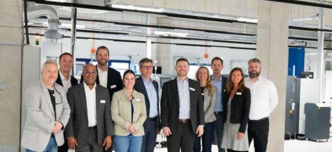
“This new manufacturing facility will support our $20 billion+ revenue ambition. Working with GF will allow us to go faster, lower the risk thresholds, and reinforce the European FD-SOI ecosystem. We will have more capacity to support our European and global customers as they transition to digitalization and decarbonization” said Jean-Marc Chery, President and CEO of STMicroelectronics. “ST is transforming its manufacturing base. We already have a unique position in our 300mm wafer fab in Crolles, France which will be further strengthened by today’s announcement. We continue to invest into our new 300mm wafer fab in Agrate (near Milan, Italy), ramping up in H1 2023 with an expected full saturation by end 2025, as well as in our vertically integrated silicon carbide and gallium nitride manufacturing.”
“Our customers are seeking broad access to 22FDX® capacity for auto and industrial applications. The new facility will include GF dedicated foundry capacity for our customers offering GF’s unique innovation and will be managed by GF personnel onsite. This jointly operated, new manufacturing capacity expansion leverages ST’s Crolles existing facility infrastructure enabling GF to accelerate our growth while benefiting from economies of scale to deliver additional capacity in a highly capital efficient manner on our differentiated 22FDX platform, that has shipped more than one billion chips. With today’s announcement, we are expanding GF’s presence within Europe’s dynamic technology ecosystem and reinforcing our position as the leading semiconductor foundry in Europe,” said Dr. Thomas Caulfield, CEO GF. “Our global footprint enables GF to not only meet our customers capacity needs but also provides them supply chain security. The partnership investment with the French government, along with our long-term customer agreements, creates the right economic model for GF’s investment.”